Sealant laminated composite, sealed semiconductor devices mounting substrate, sealed semiconductor devices forming wafer, semiconductor apparatus, and method for manufacturing semiconductor apparatus

a technology of laminated composite and semiconductor devices, which is applied in the direction of transportation and packaging, water-setting substance layered products, synthetic resin layered products, etc., can solve the problems of reducing the reliability of the semiconductor apparatus, and achieve the effects of preventing the peeling of the semiconductor device, excellent sealing characteristics, and suppressing contraction stress

Inactive Publication Date: 2014-09-18
SHIN ETSU CHEM IND CO LTD
View PDF5 Cites 5 Cited by
  • Summary
  • Abstract
  • Description
  • Claims
  • Application Information

AI Technical Summary

Benefits of technology

[0014]In addition to the above-mentioned, even when a sealing material excellent in the sealing performance such as the heat resistance and the humidity resistance is used to seal, when an ionic impurity derived from a fiber base material or an ionic impurity intruded from the outside of a semiconductor apparatus, and an ionic impurity derived from a semiconductor apparatus or a semiconductor devices mounting substrate are slightly contained in the sealing material, there is a problem in that the reliability of the semiconductor apparatus is reduced.
[0015]The invention was performed to solve the above problems. It is an object of the invention to provide a very versatile sealant laminated composite by which, even when a thin substrate or wafer having a large diameter is sealed, the substrate or the wafer can be prevented from warping and the semiconductor devices can be suppressed from peeling, the semiconductor devices mounting surface of a substrate on which semiconductor devices are mounted and the semiconductor devices forming surface of a wafer on which semiconductor devices are formed can be each collectively sealed on a wafer level, and after sealing, the sealing performance such as the heat resistance and the humidity resistance is excellent.

Problems solved by technology

In addition to the above-mentioned, even when a sealing material excellent in the sealing performance such as the heat resistance and the humidity resistance is used to seal, when an ionic impurity derived from a fiber base material or an ionic impurity intruded from the outside of a semiconductor apparatus, and an ionic impurity derived from a semiconductor apparatus or a semiconductor devices mounting substrate are slightly contained in the sealing material, there is a problem in that the reliability of the semiconductor apparatus is reduced.

Method used


Image

  • Sealant laminated composite, sealed semiconductor devices mounting substrate, sealed semiconductor devices forming wafer, semiconductor apparatus, and method for manufacturing semiconductor apparatus
  • Sealant laminated composite, sealed semiconductor devices mounting substrate, sealed semiconductor devices forming wafer, semiconductor apparatus, and method for manufacturing semiconductor apparatus
  • Sealant laminated composite, sealed semiconductor devices mounting substrate, sealed semiconductor devices forming wafer, semiconductor apparatus, and method for manufacturing semiconductor apparatus

Examples


synthesis example 1

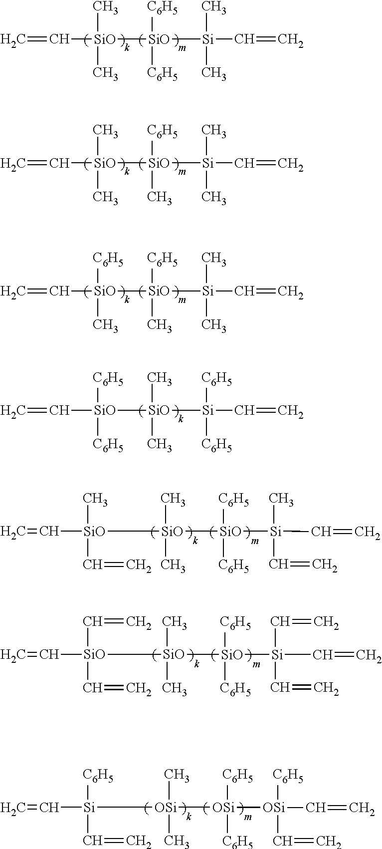
Organosilicon Compound Having Non-Conjugated Double Bond (A1)

[0128]To synthesize an organosilicon compound having a non-conjugated double bond (A1), 27 mol of organosilane represented as PhSiCl3, 1 mol of ClMe2SiO(Me2SiO)33SiMe2Cl, and 3 mol of MeViSiCl2 were dissolved in a toluene solvent, dropped into wafer, co-hydrolyzed, rinsed, neutralized by alkali cleaning, and dehydrated, and then the solvent was stripped. A composition ratio of constituent units of this compound is represented by an expression: [PhSiO3 / 2]0.27[—SiMe2o-(Me2SiO)33—SiMe2O—]0.01[MeViSiO2 / 2]0.03. A weight-average molecular weight of this compound was 62,000, and a melting point thereof was 60° C. It is to be noted that Vi in the composition formula represents a vinyl group represented by (—CH═CH2), and Me, Ph respectively represent a methyl group and a phenyl group (hereinafter, the same as the above).

Synthesis of Organohydrorgenpolysiloxane

synthesis example 2

Organohydrogenpolysiloxane (B1)

[0129]To synthesize an organohydrorgenpolysiloxane (B1), 27 mol of organosilane represented as PhSiCl3, 1 mol of ClMe2SiO(Me2SiO)33SiMe2Cl, and 3 mol of MeHSiCl2 were dissolved in a toluene solvent, dropped into wafer, co-hydrolyzed, rinsed, neutralized by alkali cleaning, and dehydrated, and then the solvent was stripped. A composition ratio of constituent units of this resin is represented by an expression: [PhSiO3 / 2]0.27[—SiMe2O-(Me2SiO)33—SiMe2O—]0.01[MeHSiO2 / 2]0.03. A weight-average molecular weight of this compound was 58,000, and a melting point of the same was 58° C.

example 1

Fabrication of Composition for Forming Uncured Resin Layer Constituted of Uncured Thermosetting Resin

[0130]With respect to a composition in which 50 parts by mass of the organosilicon compound having a non-conjugated double bond (A1), 50 parts by mass of organohydrogenpolysiloxane (B1), 0.2 parts by mass of acetylene alcohol-based ethynylcyclohexanol as a reaction inhibitor, and 0.1 parts by mass of an octyl alcohol-modified solution of a chloroplatinic acid were added, 350 parts by mass of spherical silica having an average particle size of 5 μm were added at 60° C. and well agitated by a planetary mixer heated to 60° C. to fabricate a silicone resin composition (I-a). The composition was solid at room temperature (25° C.)

[Fabrication of Sealant Laminated Composite]

[0131]The silicone resin composition (I-a) was sandwiched between a silicon wafer (support wafer) having a diameter of 300 mm (12 inches) and a fluororesin-coated PET film (release film) and compression molded for 5 min ...


PUM

PropertyMeasurementUnit
thicknessaaaaaaaaaa
thicknessaaaaaaaaaa
diameteraaaaaaaaaa

Abstract

Disclosed is a sealant laminated composite for collectively sealing a semiconductor devices mounting surface of a substrate on which semiconductor devices may be mounted or a semiconductor devices forming surface of a wafer on which semiconductor devices may be formed, including a support wafer that may be composed of silicon and an uncured resin layer that may be constituted of an uncured thermosetting resin formed on one side of the support wafer.

Description

[0001]This is a Continuation of application Ser. No. 13 / 749,289 filed Jan. 24, 2013, which claims the benefit of Japanese Patent Application No. 2012-24452 filed on Feb. 7, 2012 and Japanese Patent Application No. 2012-63158 filed Mar. 21, 2012. The disclosure of each of these prior applications is hereby incorporated by reference herein in their entireties.BACKGROUND OF THE INVENTION[0002]1. Field of the Invention[0003]The invention relates to a sealant laminated composite capable of collective seal on a wafer level, a sealed semiconductor devices mounting substrate, a sealed semiconductor devices forming wafer, a semiconductor apparatus, and a method for manufacturing a semiconductor apparatus.[0004]2. Description of the Related Art[0005]Various methods have been proposed and studied for sealing, on a wafer level, a semiconductor devices mounting surface of a substrate on which semiconductor devices are mounted, or a semiconductor devices forming surface of a wafer on which semico...

Claims


Application Information

Patent Timeline
Patent Type & Authority Applications(United States)
IPC IPC(8): H01L21/56H01L21/78H01L23/31
CPCH01L21/561H01L21/78H01L23/31H01L23/293H01L23/3135H01L24/97H01L24/32H01L2224/29099H01L2224/32225H01L2924/10253H01L2924/15788H01L2924/181H01L2924/00014H01L2924/00Y10T428/26Y10T428/24942Y10T428/269Y10T428/31663Y10T428/31504Y10T428/31511H01L21/56H01L23/29B32B27/00B32B5/00
Inventor SHIOBARA, TOSHIOAKIBA, HIDEKISEKIGUCHI, SUSUMU
Owner SHIN ETSU CHEM IND CO LTD
Why Eureka
Try Eureka