Si PRECURSORS FOR DEPOSITION OF SiN AT LOW TEMPERATURES

a technology of silicon nitride and precursors, which is applied in the direction of semiconductor/solid-state device manufacturing, basic electric elements, electric apparatus, etc., can solve the problems of affecting the production efficiency of silicon nitride films, the film deposited on the sidewalls of trenches or fins or other three-dimensional features displays inferior film properties as compared, and the structure such as these would not generally survive further processing

Active Publication Date: 2014-09-18
ASM IP HLDG BV
View PDF31 Cites 390 Cited by
  • Summary
  • Abstract
  • Description
  • Claims
  • Application Information

AI Technical Summary

Benefits of technology

[0011]In some embodiments the silicon nitride film is deposited on a three-dimensional structure. In some embodiments the silicon nitride film exhibits a step coverage and pattern loading effect of at least about 80%. In some embodiments the structure comprises a s

Problems solved by technology

Current PEALD silicon nitride processes in general suffer from anisotropic etch behavior when deposited on a three-dimensional structure, such as a trench structure.
In other words, the film deposited on the sidewalls of a trench or fin

Method used


Image

  • Si PRECURSORS FOR DEPOSITION OF SiN AT LOW TEMPERATURES
  • Si PRECURSORS FOR DEPOSITION OF SiN AT LOW TEMPERATURES
  • Si PRECURSORS FOR DEPOSITION OF SiN AT LOW TEMPERATURES

Examples


example 1

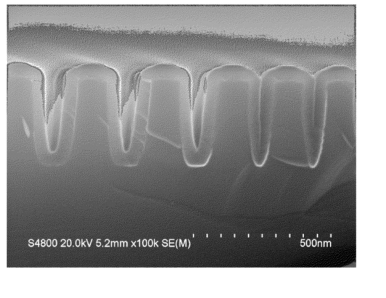
[0206]A silicon nitride thin film was deposited at 400° C. according to the present disclosure by a PEALD process using H2SiI2 as the silane precursor and H2+N2 plasma as the nitrogen precursor. This film exhibited a combination of some of the best qualities of both ALD reaction types: the typical high quality of PEALD SiN films and the isotropic etch behavior of thermal ALD films. While these results are not fully understood, the film properties and etch behavior were nevertheless within the specs for the high quality spacer layer application.

[0207]For this application, the step coverage and pattern loading effect on a trench structure with an aspect ratio of 2 should be over 95%, the wet etch rate (WER) should be less than 50% of the WER of thermally oxidized silicon (SiO2, TOX), and the etch rate should be about the same on horizontal and vertical walls of the trench structure. Finally, the growth rate should be over 0.5 nm / min and impurity contents as low as possible.

[0208]At 40...

example 2

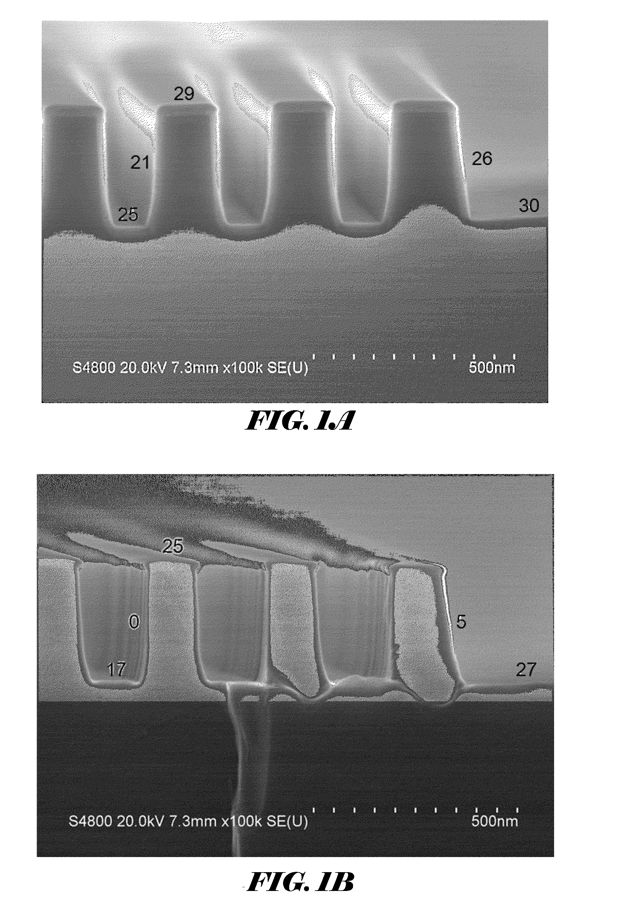
[0212]Silicon nitride thin film with improved etch properties and impurity content (compared to example 1) were deposited in a direct plasma ALD showerhead reactor by PEALD processes according to the present disclosure. Susceptor temperatures of 200° C. and 400° C. were used. H2SiI2 was used as the silicon precursor and H2+N2 plasma was used as the nitrogen precursor. Plasma power was from about 200 W to about 220 W and the gap between the showerhead plate and susceptor (i.e. the space where plasma is generated) was 10 mm. The plasma did not contain Ar. Nitrogen was used as a carrier gas and was flowed throughout the deposition process. H2SiI2 consumption was about 9.0 mg / cycle.

[0213]At 400° C. the films growth rate was 0.7 Å / cycle and the deposited films were conformal. The refractive indexes were 1.92-1.93. The wet etch rates (WER) of planar films in 100:1 dHF were from about 20 to 30% of the WER of thermal oxide (SiO2). On a trench structure the film wet etch rate ratio of trench...


PUM


Abstract

Methods and precursors for depositing silicon nitride films by atomic layer deposition (ALD) are provided. In some embodiments the silicon precursors comprise an iodine ligand. The silicon nitride films may have a relatively uniform etch rate for both vertical and the horizontal portions when deposited onto three-dimensional structures such as FinFETS or other types of multiple gate FETs. In some embodiments, various silicon nitride films of the present disclosure have an etch rate of less than half the thermal oxide removal rate with diluted HF (0.5%).

Description

BACKGROUND OF THE INVENTION[0001]1. Field of the Invention[0002]The present disclosure relates generally to the field of semiconductor device manufacturing and, more particularly, to low temperature deposition of silicon nitride films and precursors for use in deposition of silicon nitride films.[0003]2. Description of the Related Art[0004]Spacers are widely used in semiconductor manufacturing as structures to protect against subsequent processing steps. For example, nitride spacers formed beside gate electrodes can be used as a mask to protect underlying source / drain areas during doping or implanting steps.[0005]As the physical geometry of semiconductor devices shrinks, the gate electrode spacer becomes smaller and smaller. The spacer width is limited by the nitride thickness that can be deposited conformably over the dense gate electrodes lines. So the nitride spacer etching process is preferred to have a high ratio of spacer width to nitride layer thickness as deposited.[0006]Cur...

Claims


Application Information

Patent Timeline
IPC IPC(8): H01L21/02
CPCH01L21/0217H01L21/02274H01L21/02222H01L21/02211H01L21/0228H01L21/31111H01L21/823431
Inventor NISKANEN, ANTTI J.CHEN, SHANGPORE, VILJAMIFUKAZAWA, ATSUKIFUKUDA, HIDEAKIHAUKKA, SUVI P.
Owner ASM IP HLDG BV
Why Eureka
Try Eureka