Synchronized pulsed lada for the simultaneous acquisition of timing diagrams and laser-induced upsets

a timing diagram and laser technology, applied in the field of laser-based defect localization analysis of integrated circuits, can solve the problems of imposing the limitation on further improvement of the single photon lada spatial resolution, the inability to improve the spatial resolution of the single photon lada system by the use of smaller wavelength lasers, etc., to achieve enhanced spatial resolution, high spatial resolution of fault localization, and sufficient energy

Active Publication Date: 2014-09-25
DCG SYST +1
View PDF9 Cites 8 Cited by
  • Summary
  • Abstract
  • Description
  • Claims
  • Application Information

AI Technical Summary

Benefits of technology

[0014]Various embodiments disclosed enable higher spatial resolution of fault localization by utilizing time domain to enable enhanced spatial resolution. Disclosed embodiments utilize a pulsed laser with sufficient energy in lieu of a continuous wave laser. The pulsed laser is synchronized to the device's clock, thus enabling improved spatial resolution. Various embodiments utilize a 1064 nm wavelength laser for a single-photon LADA, or longer wavelengths so as to exploit the non-linear two-photon absorption mechanism to induce LADA effects. This later technique is referred to herein as Two-Photon Laser Assisted Device Alteration technique (2pLADA).
[0015]Disclosed embodiments enable fault localization by using test vectors stimulating a DUT and at the same time use a femtosecond, a pico-second, or even a nano-second pulsed laser to scan an area of interest in the DUT and examine the response of the DUT to the test vectors during the scan. The laser source is chosen such that the wavelength provides photon energy below the band gap of silicon and it provides pulses of femtosecond pulse width. The pulse widths for optimum resolution relates to device operating frequency. A clock signal is obtained from the ATE and is fed to the DUT and to the circuit controlling the pulsed laser. The timing of the pulses can be shifted relative to the ATE clock, so as to investigate the pass / fail characteristics of various devices. Additionally, by using proper synchronization of the laser pulses to the clock, spatial resolution is enhanced to enable resolving multiple devices, i.e., transistors, within the laser beam.

Problems solved by technology

The limitation on further improvement of the single photon LADA spatial resolution is imposed by the laser light wavelength.
However, optical absorption of silicon at wavelength smaller than 1064 nm prevents the use of shorter wavelengths, as it becomes the major obstacle for delivering light to the transistor through the backside.
Thus, while design rules of modern devices shrink, the spatial resolution of the LADA system cannot be improved by the use of smaller wavelength laser.
For example, at 22 nm design rule it is doubtful that conventional LADA will be able to resolve among four neighboring transistors.

Method used


Image

  • Synchronized pulsed lada for the simultaneous acquisition of timing diagrams and laser-induced upsets
  • Synchronized pulsed lada for the simultaneous acquisition of timing diagrams and laser-induced upsets
  • Synchronized pulsed lada for the simultaneous acquisition of timing diagrams and laser-induced upsets

Examples


examples

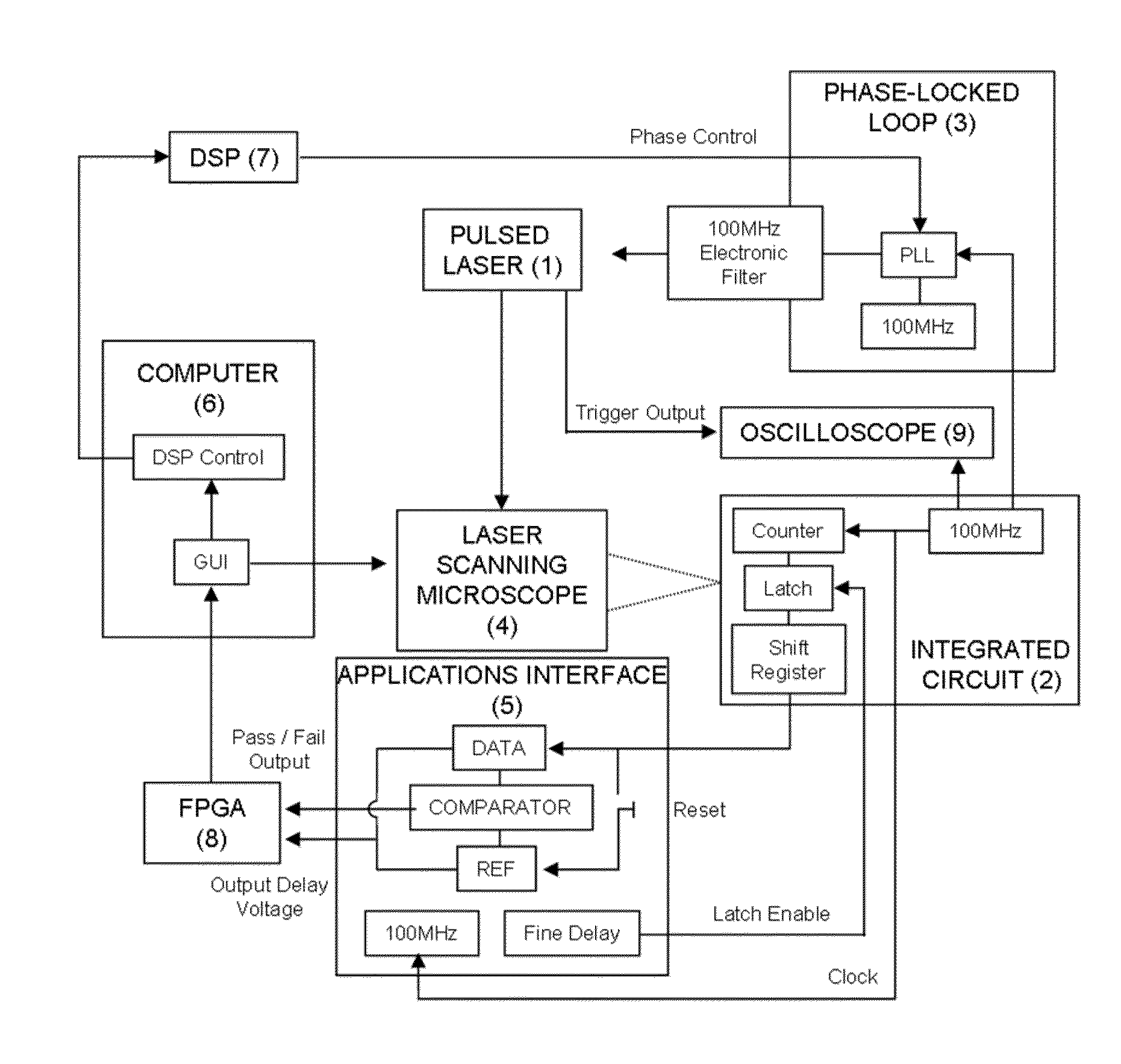
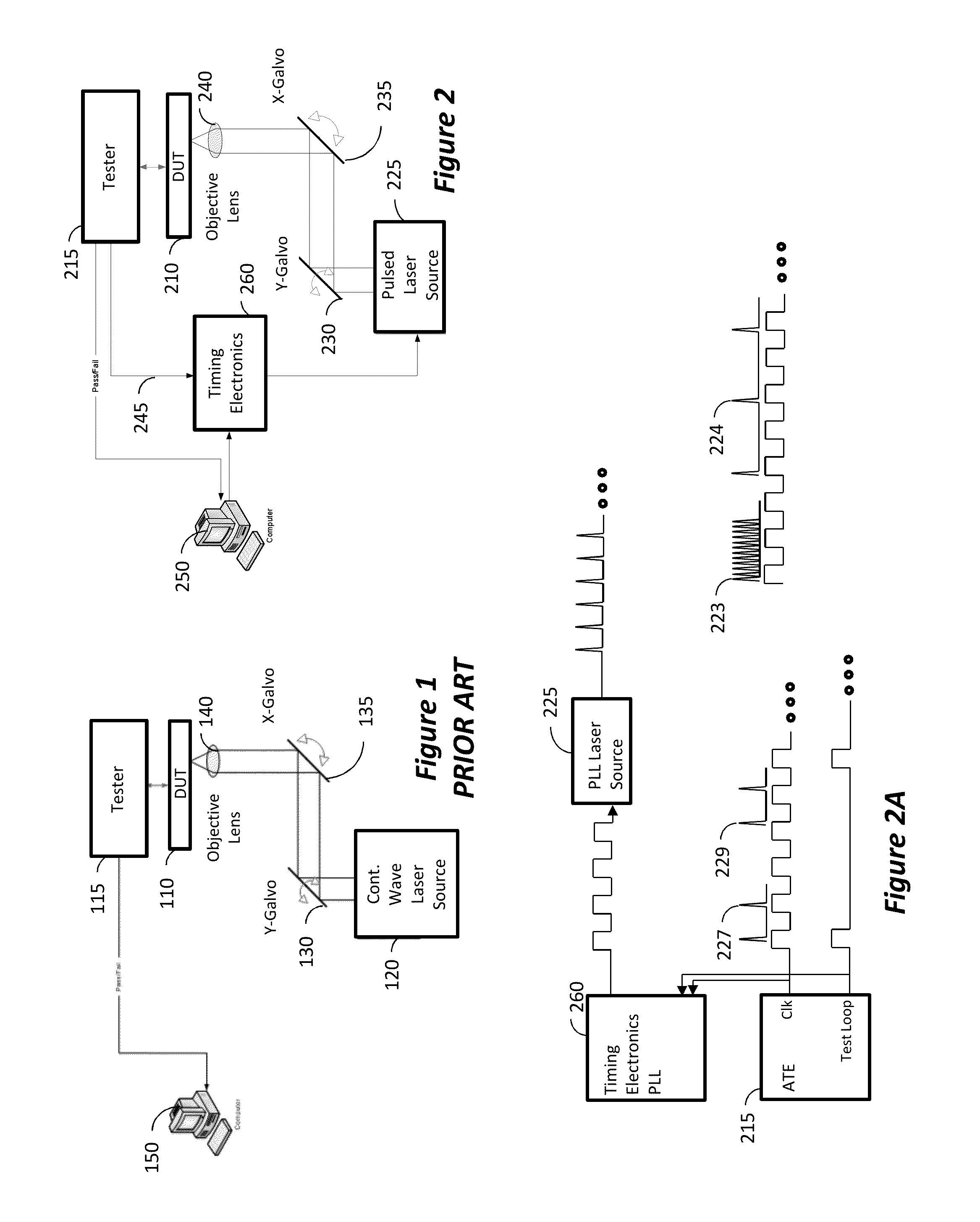
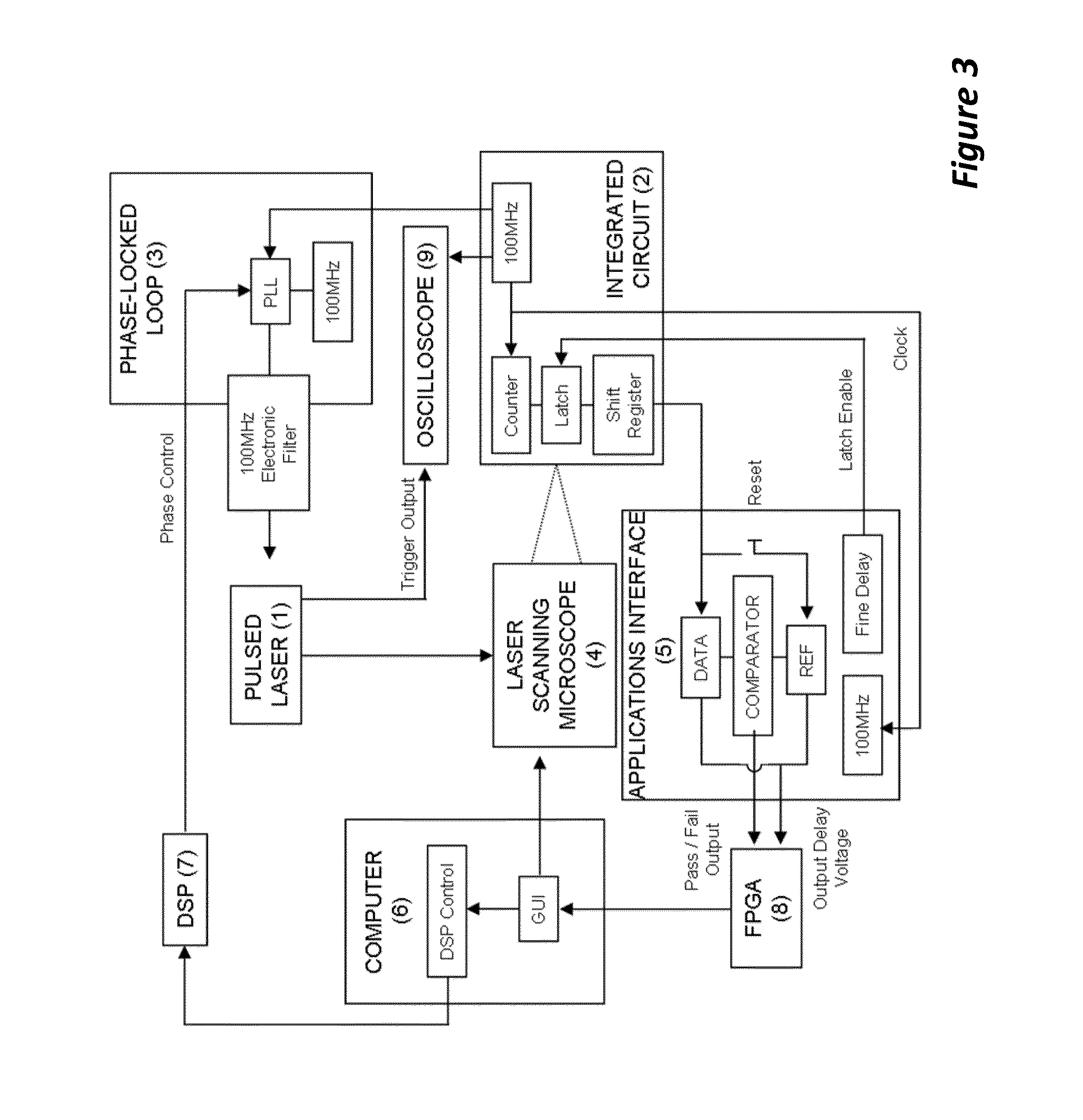
[0064]Constructing a pulsed LADA system with a pulsed optical source allows for novel aspects of the operating device to be evaluated and measured. When traditional single-photon or alternative two-photon LADA utilize a CW laser, the optical radiation is constantly interacting with the individual transistors with a potentially damaging level of invasiveness. A pulsed LADA methodology, on the other hand, allows the switching characteristics of the individual transistors to be mapped out in as much as two-physical dimensions. Extended pulsed LADA concepts are discussed in detail below.

[0065]Under conventional CW LADA stimulation, device theory and practice informs us that the magnitude of laser-induced device perturbations from a p-type metal-oxide-semiconductor (PMOS) transistor dominates over its n-type (NMOS) neighbor. Since the diameter of the laser beam would cover both the p-type and its neighboring n-type transistors, the resulting spatial resolution is insufficient to distingu...


PUM


Abstract

Method to extract timing diagrams from synchronized single- or two-photon pulsed LADA by spatially positioning the incident laser beam on circuit feature of interest, temporally scanning the arrival time of the laser pulse with respect to the tester clock or the loop length trigger signal, then recording the magnitude and sign of the resulting fail rate signature per laser pulse arrival time. A Single-Photon Laser-Assisted Device Alteration apparatus applies picosecond laser pulses of wavelength having photon energy equal to or greater than the silicon band-gap. A Two-Photon Laser-Assisted Device Alteration apparatus applies femtosecond laser pulses of wavelength having photon energy equal to or greater than half the silicon band-gap at the area of interest. The laser pulses are synchronized with test vectors so that pass/fail ratios can be altered using either the single-photon or the two-photon absorption effect. A sequence of synthetic images with error data illustrates timing sensitive locations.

Description

CROSS-REFERENCE TO RELATED APPLICATIONS[0001]This application claims priority benefit from U.S. Provisional Application No. 61 / 804,696, filed on Mar. 24, 2013; from U.S. Provisional Application No. 61 / 806,803, filed on Mar. 29, 2013; and from U.S. Provisional Application No. 61 / 838,679, filed on Jun. 24, 2013; the disclosures of which are incorporated herein by reference in their entirety.GOVERNMENT LICENSE RIGHTS[0002]This invention is based upon work supported by the Office of the Director of National Intelligence (ODNI), Intelligence Advanced Research Project Activity (IARPA), via Air Force Research Laboratory (AFRL) contract number FA8650-11-C-7104. The ideas and conclusions contained herein are those of the inventors and should not be interpreted as necessarily having the official endorsements, either expressed or implied, of ODNI, IARPA, AFRL, or the U.S. Government.BACKGROUND[0003]1. Field of Invention[0004]This invention is in the field of laser-based defect localization ana...

Claims


Application Information

Patent Timeline
Patent Type & Authority Applications(United States)
IPC IPC(8): G01R31/311
CPCG01R31/311
Inventor SERRELS, KEITHVEDAGARBHA, PRAVEENLUNDQUIST, TEDERINGTON, KENTBODOH, DAN
Owner DCG SYST
Why Eureka
Try Eureka