Memory system

a memory system and memory technology, applied in the field of memory systems, can solve the problems of inability to perform burst reading, inconvenient file recording, and small writing bandwidth

Active Publication Date: 2014-09-25
KIOXIA CORP
View PDF3 Cites 192 Cited by
  • Summary
  • Abstract
  • Description
  • Claims
  • Application Information

AI Technical Summary

Benefits of technology

[0017]the control circuit functions to read data from a desired target area to-be-determined of the flash-EEPROM nonvolatile memory and detect an erased area to determine a written area / unwritten area by using as a determination condition whether or not a count number of data “0” of the read data has reached a preset criterion count number.

Problems solved by technology

However, since the effective bandwidth of writing is small, it is not suitable for file recording.
Further, burst reading can be performed and the effective bandwidth is large.
However, since the number of bits that can be simultaneously programmed or erased is large, write data can be taken in by a burst operation and a large number of bits can be simultaneously programmed in units of pages, the effective bandwidth becomes large.
However, there are some restrictions on usage.
First, since data degradation occurs due to writing / erasing (programming / erasing), there are restrictions on the number of writable / erasable operations.
If the above operations are repeatedly performed, an oxide film around the floating gate of the memory cell transistor is degraded and data is destroyed.
However, if the NAND flash memory is mounted in a system and used instead of a hard disk, accesses of approximately 105 times will occur in a relatively short period of time.

Method used


Image

  • Memory system
  • Memory system
  • Memory system

Examples


first embodiment

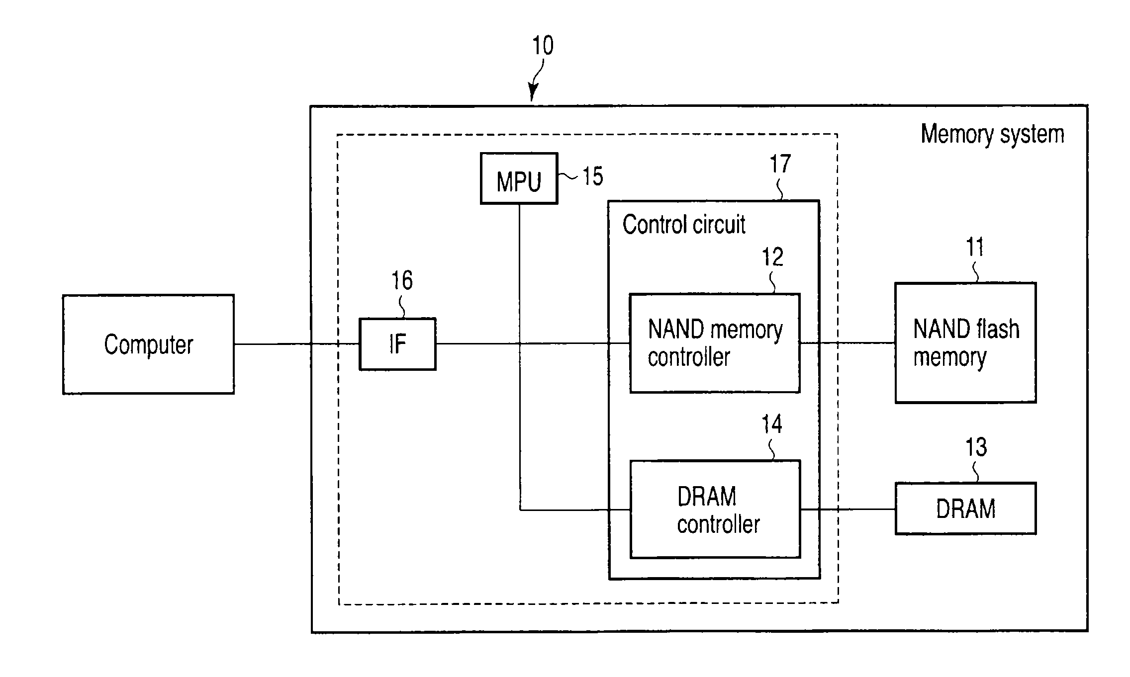
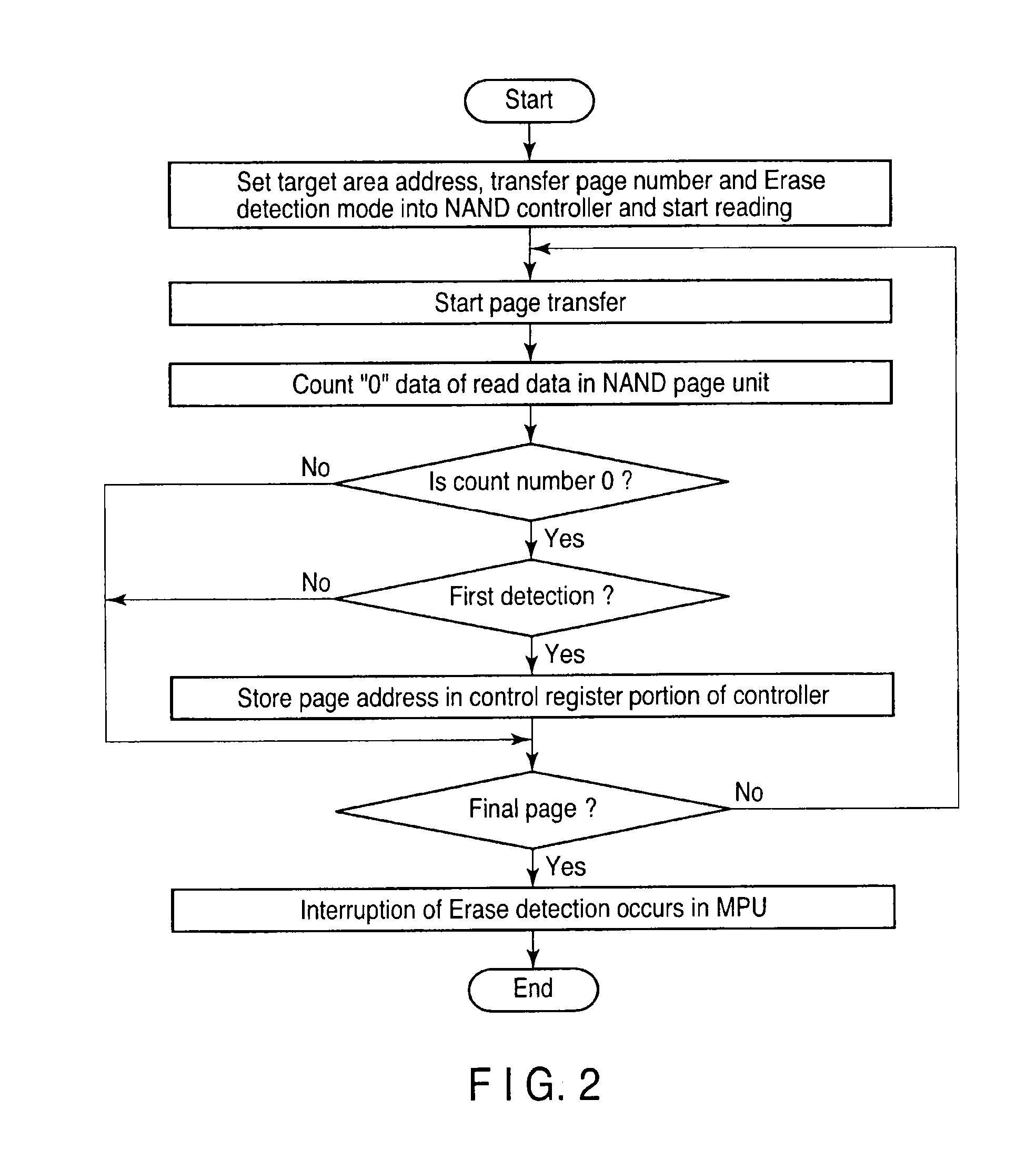
[0030]FIG. 1 is a block diagram showing a memory system according to a first embodiment of the present invention. FIG. 2 shows one example of a flowchart of processing steps in the memory system of FIG. 1. FIG. 3 shows part of the configuration of the memory system of FIG. 1 and one example of a data processing operation.

[0031]As shown in FIG. 1, a memory system 10 includes a flash-EEPROM (electrically erasable and programmable read only memory) nonvolatile memory (in this example, NAND flash memory) 11 having a plurality of memory cells each of which has a floating gate and in which data can be electrically erased and written, a cache memory (in this example, DRAM (dynamic random access memory)) 13 that temporarily stores data of the NAND flash memory 11, a control circuit 17 (NAND memory controller 12, DRAM controller 14) that controls the above two types of memories, an MPU (micro processor unit) 15, and an interface circuit IF 16 that communicates with a host computer. The NAND ...

second embodiment

[0039]FIG. 4 shows one example of a flowchart of processing steps in a memory system of a second embodiment of the present invention. In comparison with the memory system of the first embodiment described before, the memory system adds a function of immediately interrupting transfer of erased page detection to the DRAM 13 and reading from the NAND flash memory 11 in a case where an erased page is detected in the same block when the number of data items “0” is counted while transferring data of a target area in which an erased page is to be detected to the DRAM 13 to a sequencer 35 (FIG. 3).

[0040]Determination of validity / invalidity of write data can be made when an erased page is detected and since data after detection of the erased page is invalid data (erased data), it is not necessary to transfer the data to the DRAM 13. With this function, the extra data transfer time can be omitted and a processing time required in the system can be shortened.

third embodiment

[0041]FIG. 5 shows one example of a flowchart of processing steps in a memory system of a third embodiment of the present invention. FIG. 6 shows part of the configuration of the memory system of the third embodiment and one example of a data processing operation.

[0042]In the memory system of the first or second embodiment, the count number of data “0” is set to a value not smaller than one as a determination condition when the number of data “0” is counted while transferring data of an area in which an erased page is to be detected to the DRAM 13. In a NAND flash memory, it is common practice to use an error correction (ECC: error check and correction) circuit to take a countermeasure against aging deterioration of data and deterioration of cells accompanied by an increase in the number of writings during the operation. In this case, the data of a portion of each erased page may be set to “0” data even if the erase process is performed.

[0043]Therefore, in the memory system of the t...


PUM


Abstract

A memory system (10) is disclosed, which comprises a flash-EEPROM nonvolatile memory (11) having a plurality of memory cells that have floating gates and in which data items are electrically erasable and writable, a cache memory (13) that temporarily stores data of the flash-EEPROM nonvolatile memory (11), a control circuit (12, 14) that controls the flash-EEPROM nonvolatile memory (11) and the cache memory (13), and an interface circuit (16) that communicates with a host, in which the control circuit functions to read data from a desired target area to-be-determined of the flash-EEPROM nonvolatile memory and detect an erased area to determine a written area / unwritten area by using as a determination condition whether or not a count number of data “0” of the read data has reached a preset criterion count number.

Description

CROSS-REFERENCE TO RELATED APPLICATIONS[0001]This application is a Divisional of and claims the benefit of priority under 35 U.S.C. §120 from U.S. application Ser. No. 12 / 529,473, filed Sep. 1, 2009, which is the U.S. national phase application under 35 U.S.C. §371 of international application PCT / JP2009 / 054375 (not published in English), filed Mar. 3, 2009, and claims priority to Japanese patent application no. 2008-058549 filed on Mar. 7, 2008, the entire contents of each of which are incorporated herein by reference.TECHNICAL FIELD[0002]This invention relates to a memory system using a flash-EEPROM nonvolatile memory, and more particularly to a memory system that uses a NAND flash memory having an ascending-order programming restriction and is used instead of a hard disk device, for example.BACKGROUND ART[0003]At present, semiconductor memories are used in various devices, including main memory devices of large-scale computers, personal computers, home electrical appliances, mobi...

Claims


Application Information

Patent Timeline
Patent Type & Authority Applications(United States)
IPC IPC(8): G06F11/10G06F12/02
CPCG06F12/0246G06F11/1016G06F2212/7203G06F2212/7209G11C16/102G06F12/00G06F12/02
Inventor NAGADOMI, YASUSHITAKASHIMA, DAISABUROHATSUDA, KOSUKE
Owner KIOXIA CORP
Why Eureka
Try Eureka