Thin-film transistor, method for manufacturing the same and display device including the same

Active Publication Date: 2014-10-02
LG DISPLAY CO LTD
View PDF5 Cites 12 Cited by
  • Summary
  • Abstract
  • Description
  • Claims
  • Application Information

AI Technical Summary

Benefits of technology

[0007]Accordingly, an improved thin-film transistor is provided. In an embodiment, a thin-film transistor according to an exemplary embodiment of the present invention may include a substrate, and an active layer formed on the substrate. The active layer may be made from a semiconductor. A gate electrode may be formed above the active layer or below the active layer. A conductive layer may come in contact with the active layer, may be overlapped with at least a part of the gate electrode, and may be insulated from the gate electrode. A source e

Problems solved by technology

Typically, the current driving ability of the thin-film transistor (TFT) deteriorates as the channel lengt

Method used


Image

  • Thin-film transistor, method for manufacturing the same and display device including the same
  • Thin-film transistor, method for manufacturing the same and display device including the same
  • Thin-film transistor, method for manufacturing the same and display device including the same

Examples


Embodiment Construction

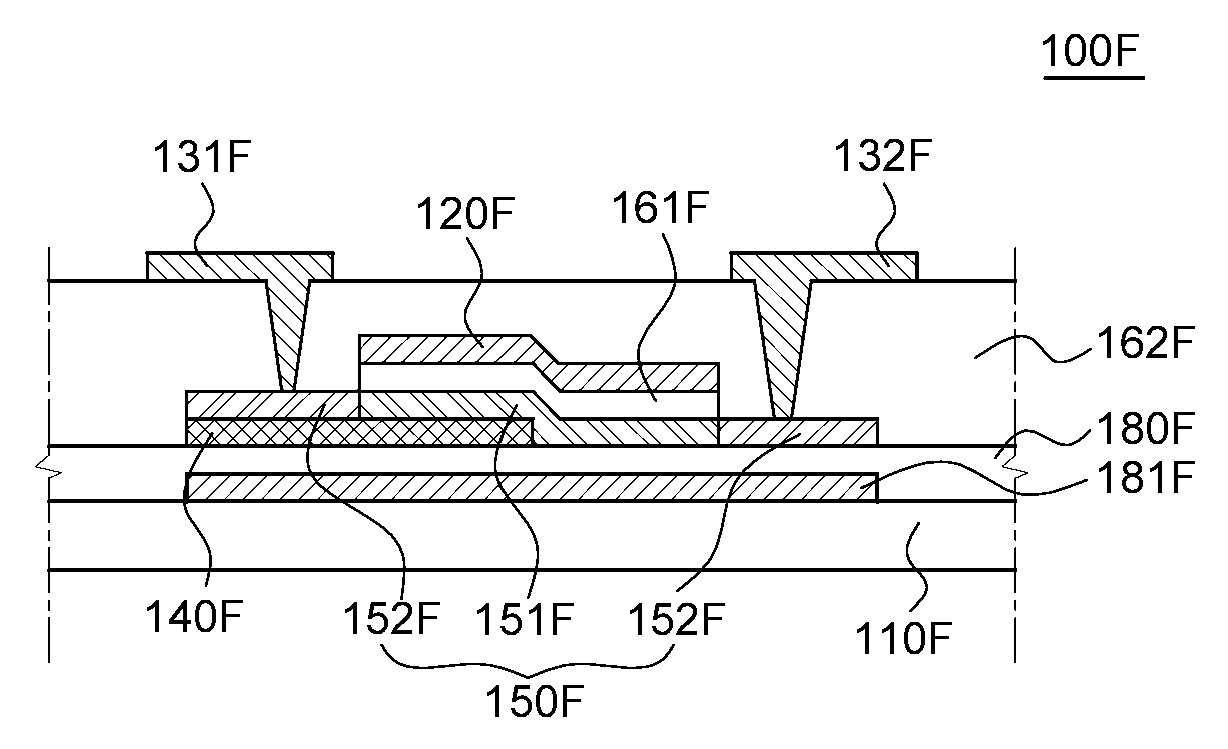
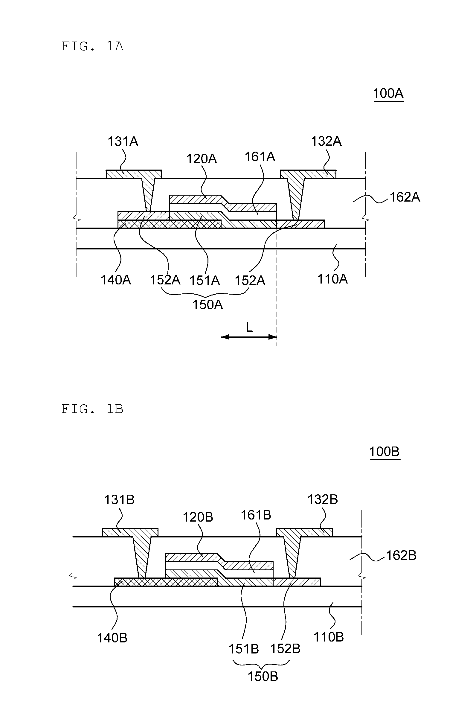
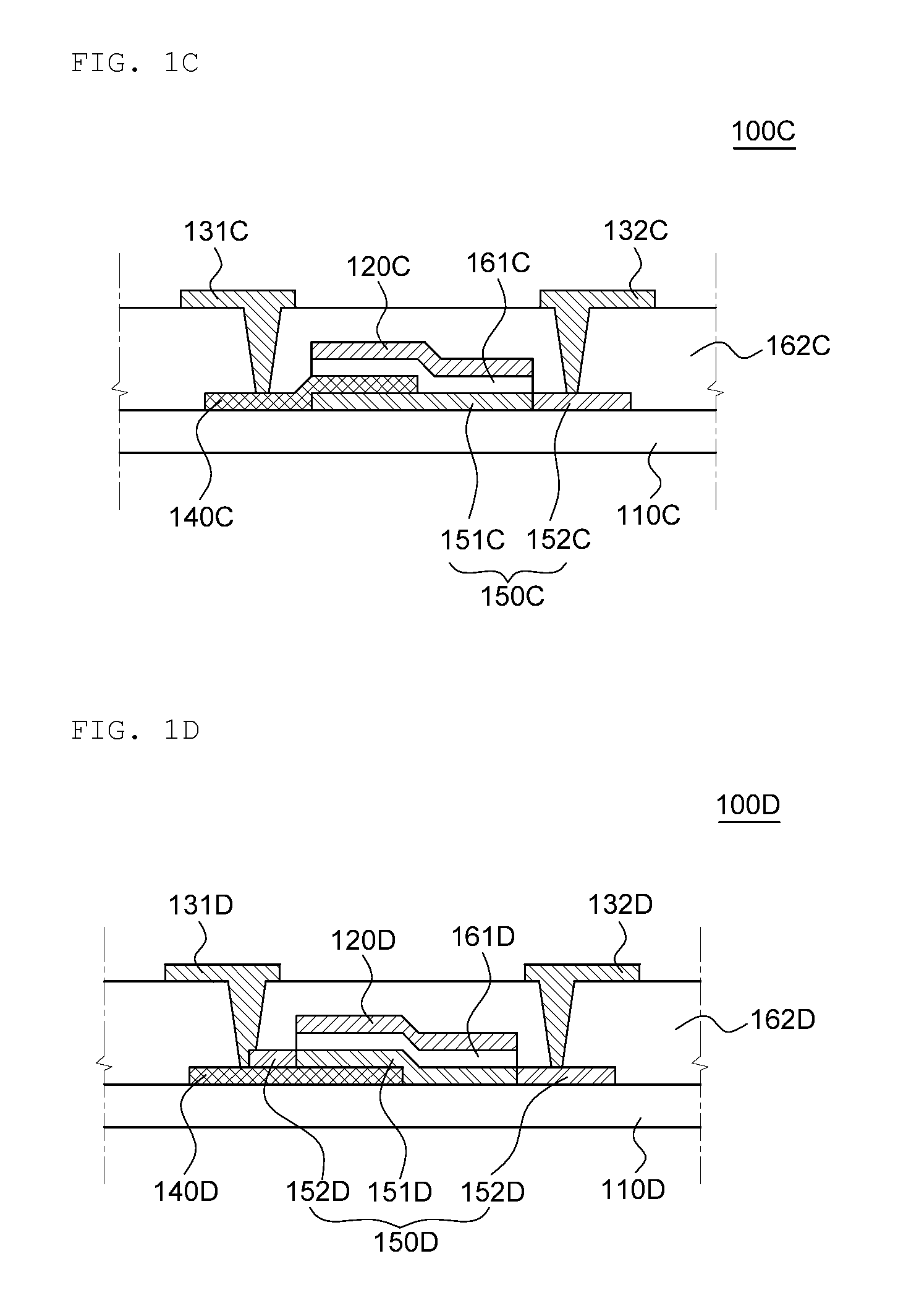
[0017]Exemplary embodiments of the present invention will be described in detail below with reference to the accompanying drawings. While the present invention is shown and described in connection with exemplary embodiments thereof, it will be apparent to those skilled in the art that various modifications can be made without departing from the scope of the invention.

[0018]An element or layer disposed or formed “on” another element or layer includes all a case in which an element is formed in direct physical contact with another element, as well as cases in which an element is indirectly physically connected with another element with one or more additional elements or layers formed therebetween.

[0019]The term “electrically connected” refers to two different elements or layers that are in direct physical contact or are indirectly connected through one or more intervening elements or layers such that an electrical current is capable of flowing between the two different elements or lay...


PUM


Abstract

A thin-film transistor, a method for manufacturing the same and a display device including the same are provided. The thin-film transistor may include a substrate, and an active layer formed on the substrate. The active layer may be made from an oxide semiconductor. A gate electrode may be formed above the active layer or below the active layer. A conductive layer may come in contact with the active layer, may be overlapped with at least a part of the gate electrode, and may be insulated from the gate electrode. A source electrode and a drain electrode may be electrically connected to the active layer. The conductive layer can reduce a channel length of the thin-film transistor and increase a capacitance between the source electrode and the gate electrode or between the drain electrode and the gate electrode.

Description

CROSS-REFERENCE TO RELATED APPLICATIONS[0001]This application claims the priority of Korean Patent Application No. 10-2013-0034429 filed on Mar. 29, 2013, in the Korean Intellectual Property Office, the disclosure of which is incorporated herein by reference.BACKGROUND OF THE INVENTION[0002]1. Field of the Invention[0003]The present invention relates to a thin-film transistor, a method for manufacturing the thin-film transistor and a display device including the thin-film transistor, and more particularly, to a thin-film transistor capable of improving driving characteristics, a method for manufacturing the thin-film transistor and a display device including the thin-film transistor.[0004]2. Description of the Related Art[0005]Recently, with growing interest in information displays and an increasing demand for portable electronic devices, light and thin-film type flat panel display (FPD) devices have been widely studied and commercialized. In particular, among the flat panel display...

Claims


Application Information

Patent Timeline
IPC IPC(8): H01L29/786H01L29/66H01L27/32
CPCH01L29/78618H01L29/66969H01L27/3265H01L27/3262H01L29/41733H01L29/7869H01L29/78696H10K59/1216H10K59/1213G02F1/136213H01L27/1255
Inventor CHO, HYUNGNYUCK
Owner LG DISPLAY CO LTD
Why Eureka
Try Eureka