

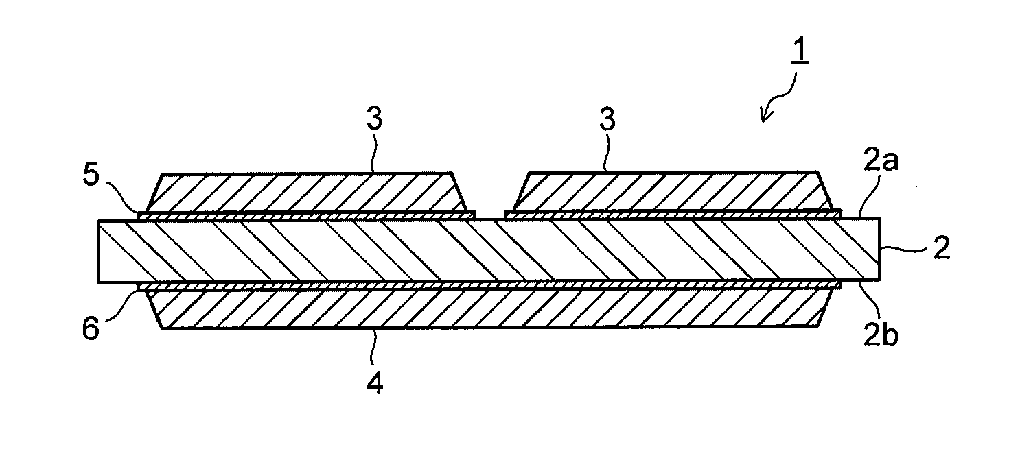
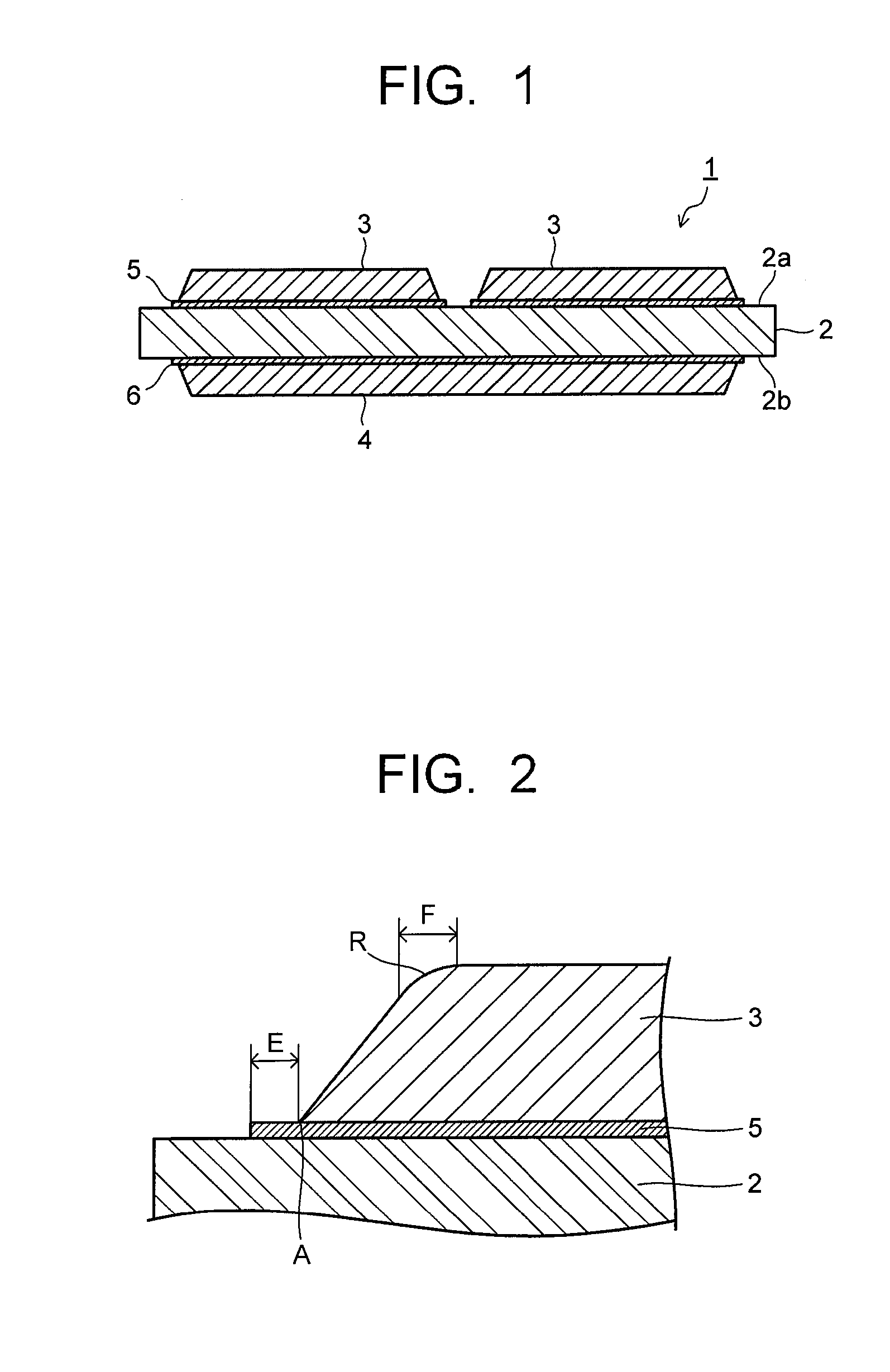
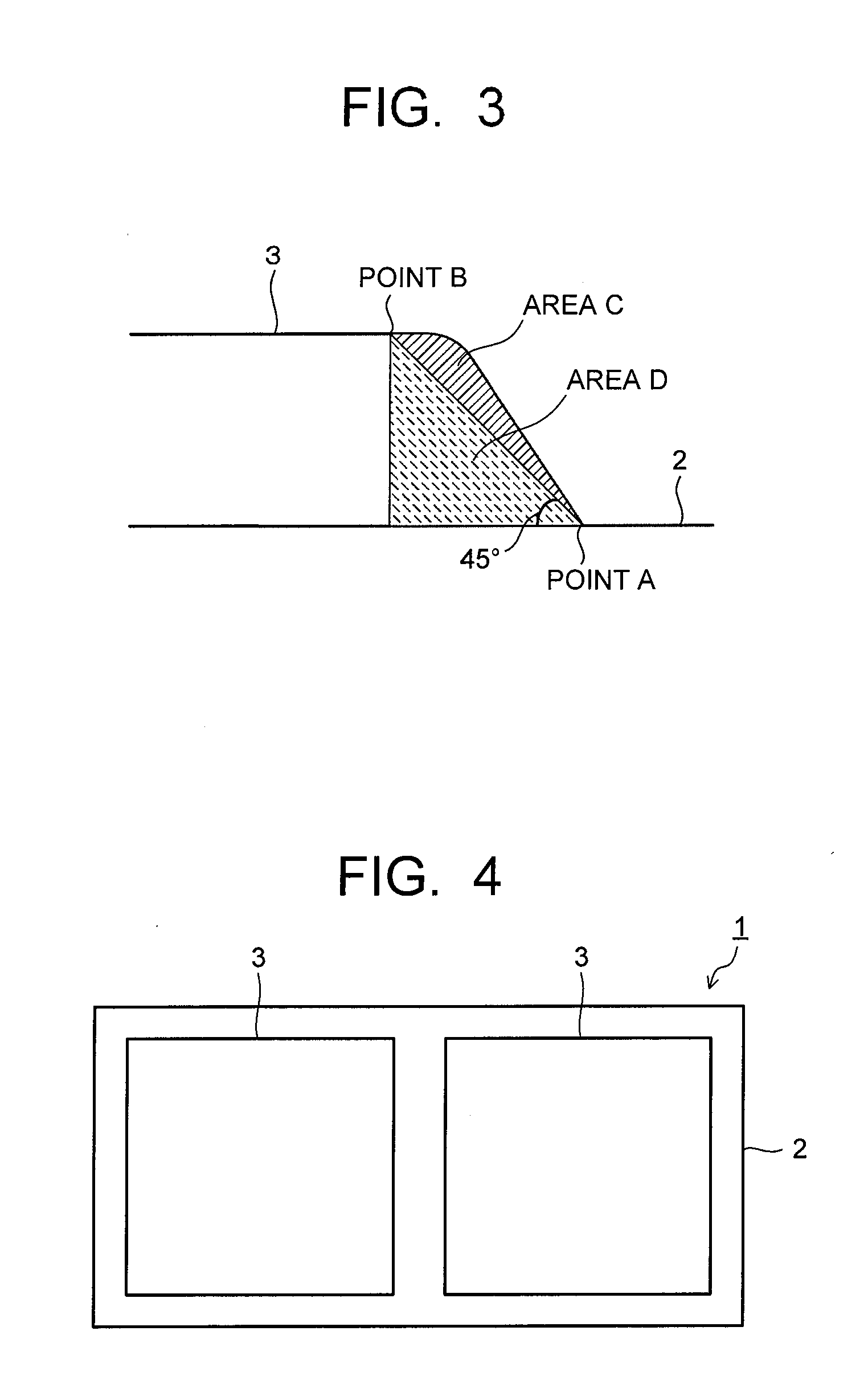
Ceramic/copper circuit board and semiconductor device
a ceramic/copper circuit board and copper plate technology, applied in the direction of semiconductor/solid-state device details, metal adhesion improvement of insulating substrates, transportation and packaging, etc., can solve the problem of reducing the detection accuracy of the copper plate end portion by the detector, the cost of silicon nitride substrates is generally more expensive, and the manufacturing cost of ceramic/copper circuit boards is increased
- Summary
- Abstract
- Description
- Claims
- Application Information
AI Technical Summary
Benefits of technology
Problems solved by technology
Method used
Image

Examples
example 1 to 11
, COMPARATIVE EXAMPLES 1 TO 9
[0042]As ceramic substrates, there are prepared a silicon nitride substrate (thermal conductivity: 90 W / m·K, three-point bending strength: 730 MPa) with a plate thickness of 0.635 mm, an aluminum nitride substrate (thermal conductivity: 180 W / m·K, three-point bending strength: 400 MPa) with a plate thickness of 0.635 mm, and an aluminum oxide substrate (thermal conductivity: 15 W / m·K, three-point bending strength: 500 MPa) with a plate thickness of 0.635 mm. Shapes of the ceramic substrates are standardized at 50 mm vertically×30 mm horizontally.
[0043]Next, an active metal brazing material whose composition is shown in Table 1 is prepared, made into a paste state, and applied onto the ceramic substrate. An application thickness of the active metal brazing material paste is shown in Table 1. Next, there is prepared a copper plate (oxygen-free copper plate) with a plate thickness of 0. 3 mm. A shape of the copper plates is standardized at 45 mm vertically×...
examples 12 , 13
EXAMPLES 12, 13
[0049]An example 12 is the ceramic copper substrate of the example 9, and an example 13 is a ceramic copper substrate whose copper plate thickness is changed to 0.5 mm from the example 9. For the ceramic / copper circuit boards of the example 12 and the example 13, TCT's are carried out under the condition 2 (one cycle: −40° C.×30 minutes→room temperature (25° C.)×10 minutes→175° C.×30 minutes→room temperature (25° C.)×10 minutes), and the number of cycles where a crack occurs in the ceramic substrate is investigated. A result thereof is shown in Table 4.
TABLE 4Cycle number where crackoccurs in ceramic substrateExample 126300Example 136100
[0050]As is known from Table 4, the ceramic / copper circuit boards of the examples have durabilities of 6000 cycles or more even in the TCT's whose maximum temperatures exceed 170° C.
examples 14 to 18
[0051]As ceramic substrates, ones described below are prepared. A ceramic substrate 1 is a silicon nitride substrate (thermal conductivity: 93 W / m·K, three-point bending strength: 700 MPa) with a plate thickness of 0.320 mm. A ceramic substrate 2 is a silicon nitride substrate (thermal conductivity: 100 W / m·K, three-point bending strength: 600 MPa) with a plate thickness of 0.320 mm. A ceramic substrate 3 is an aluminum nitride substrate (thermal conductivity: 200 W / m·K, three-point bending strength: 320 MPa) with a plate thickness of 0.635 mm. A ceramic substrate 4 is an aluminum oxide substrate (thermal conductivity: 12 W / m·K, three-point bending strength: 400 MPa) with a plate thickness of 0.635 mm. Note that shapes of the ceramic substrates are standardized at 50 mm vertically×30 mm horizontally.
[0052]Next, an active metal brazing material whose composition is shown in Table 5 is prepared, made to a paste state, and printed and applied onto the ceramic substrate. A copper plate ...
PUM
| Property | Measurement | Unit |
|---|---|---|
| lengths | aaaaa | aaaaa |
| lengths | aaaaa | aaaaa |
| thicknesses | aaaaa | aaaaa |
Abstract
Description
Claims
Application Information