
Imaging optical system and imaging equipment

Active Publication Date: 2014-10-02
SASAYA TOSHIHIRO
View PDF3 Cites 14 Cited by
  • Summary
  • Abstract
  • Description
  • Claims
  • Application Information

AI Technical Summary

Benefits of technology

The patent text describes a new imaging optical system and equipment that can use small and lightweight solid-state imaging devices. This system has a large field of view and is cost-effective and highly productive.

Problems solved by technology

However, since the imaging lens as disclosed in Japanese Patent No. 3929479 and Japanese Patent No. 3946245 is a hybrid type lens in which a plane parallel glass plate or a glass lens close to the plane parallel plate is used as a base in a lens system, the shape of the whole lens system is restricted by a base glass shape.
Accordingly, for example, it is difficult to form the lens system as a wide lens having a short focal length.
While a wider field angle is realized by arranging a glass lens having a strong power on the front side of a hybrid type lens in Japanese Patent Laid Open No. 2012-113149, the glass lens for realizing a wider field angle has a large thickness and a small radius of curvature and is difficult to manufacture, and the shape of the hybrid type lens has a large amount of sag and is also difficult to be manufactured.
However, in Japanese Patent Laid Open No. 1997-015492, a surface having a small radius of curvature and a strong curvature is used on the image plane side of each lens, and thus tolerance becomes severe, aberration is also easily caused, and compactness is lost.
In addition, the correction of the aberration such as color aberration is not sufficient because of a configuration using a single glass material.
In addition, Japanese Patent Laid Open No. 2009-063877 makes great use of a surface having a small radius of curvature for a concave lens or a cemented lens surface, and thus tolerance becomes severe and also aberration is easily caused.
Thickness differences among the respective constituent lenses are large and also there exists a lens with a lens thickness almost close to a lens outer diameter thereof, and thus it is not possible to deal with the wafer level lens manufacturing.
Furthermore, in Japanese Patent Laid Open No. 2010-107820, a glass material having a high optical index is used for the first lens and the like, and thus manufacturing cost is increased.
In addition, a relatively high power is provided to each lens, and thus aberration changes significantly among the lenses, and tolerance is severe and also aberration is easily caused.
Moreover, in Japanese Patent Laid Open No. 2012-053384, while compactness and low-cost production are considered to be possible, the field angle of a target optical system is small, and when the field angle is tried to be increased, the power of each lens becomes stronger with respect to the power of the whole lenses and also the radius of curvature of a constituent surface becomes small, resulting in a large aberration.
However, when the distribution of the lens power 1 / fq is moved largely, a surface having a strong power comes to exist, and various aberrations are easily generated and the manufacturing of the surface becomes difficult.
In particular, when a surface having a small radius of curvature and a strong power exists, it becomes difficult to deal with the wafer-level manufacturing method.
Furthermore, while the petzval sum can be reduced by the use of an optical material having an optical index higher than that of a typical material, as an optical index nq of the optical system, it is difficult to manufacture the lens at a low cost because the cost of the material is increased.

Method used


Image

  • Imaging optical system and imaging equipment
  • Imaging optical system and imaging equipment
  • Imaging optical system and imaging equipment

Examples


first embodiment

[0050]Hereinafter, an imaging optical system according to a first embodiment according to some implementations will be explained with reference to the drawings.

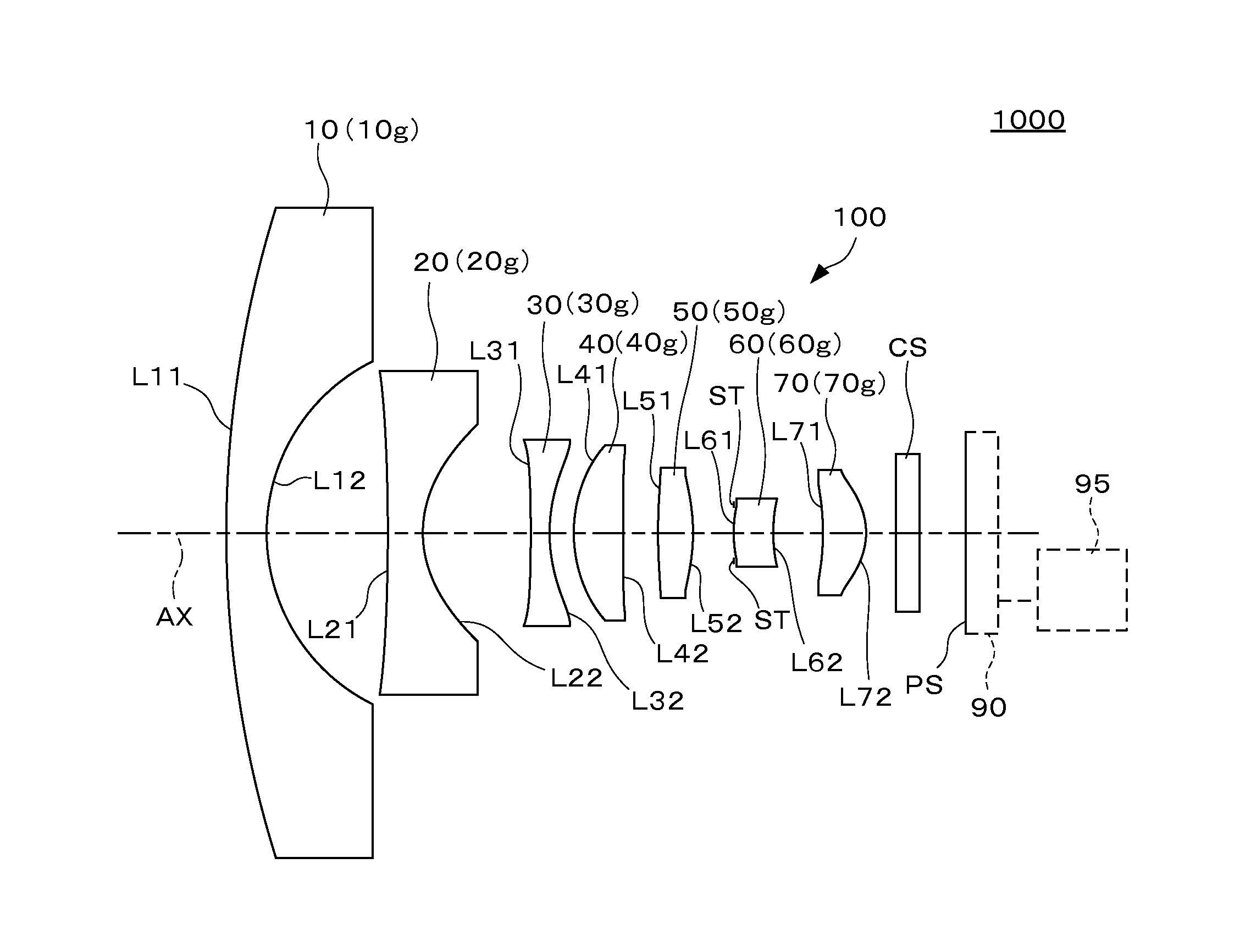
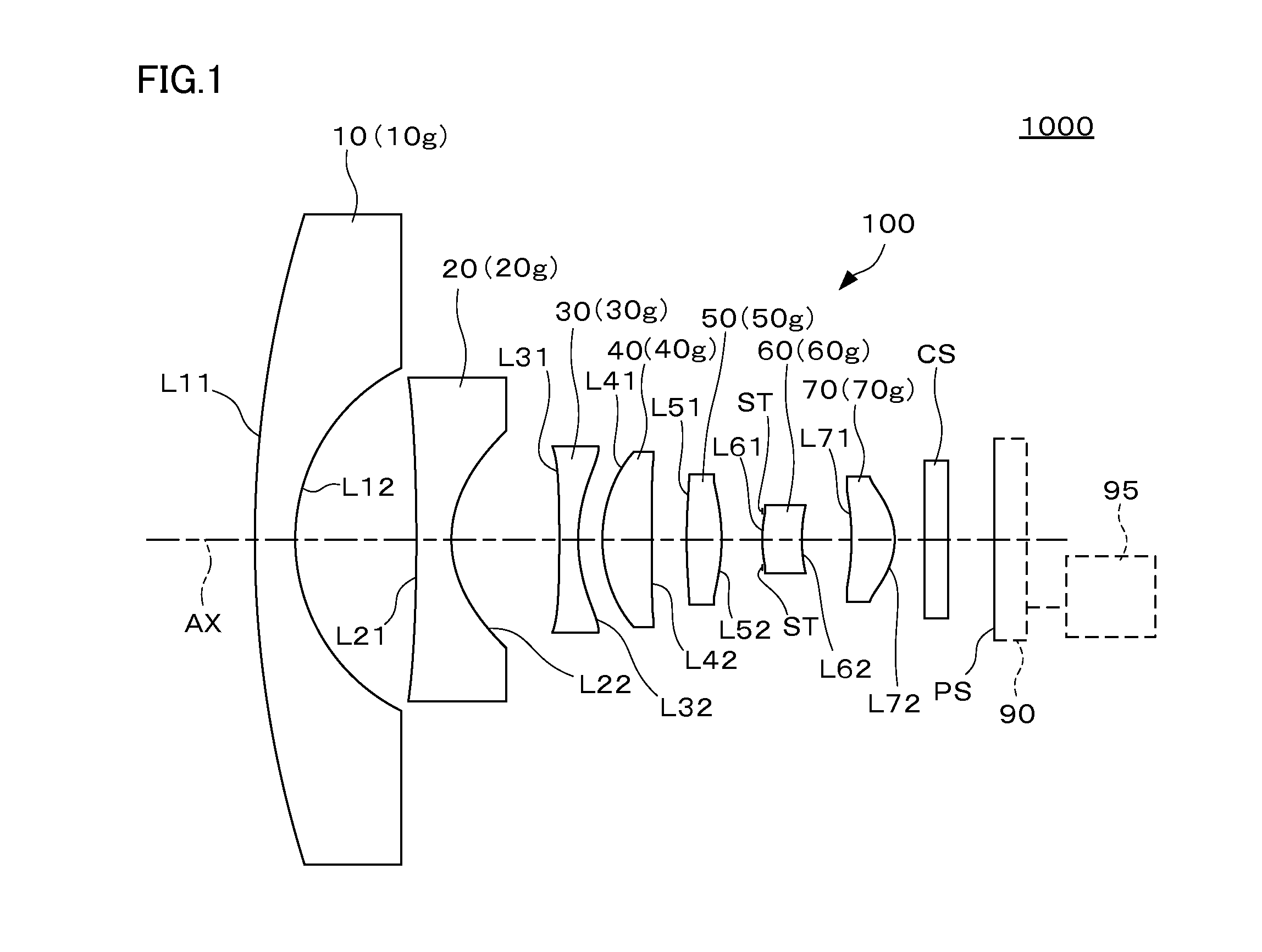
[0051]An imaging optical system 100 shown in FIG. 1 is incorporated into imaging equipment 1000 mounted in an action camera, a car-mounted camera (rearview camera), a monitoring camera, or the like, and projects an image on an object onto an imaging device 90. Here, as the imaging device 90, such an imaging equipment 1000 uses a solid-state imaging device such as a compact CCD image sensor and a compact CMOS image sensor having a size of ½ inches or less. Meanwhile, the imaging device 90 performs an imaging action according to a drive signal from a drive circuit 95.

[0052]As shown in FIG. 1, the imaging optical system 100 is provided with the first lens 10, second lens 20, third lens 30, fourth lens 40, fifth lens 50, sixth lens 60, seventh lens 70, and an aperture stop ST which are arranged sequentially from the object side (...

example 1

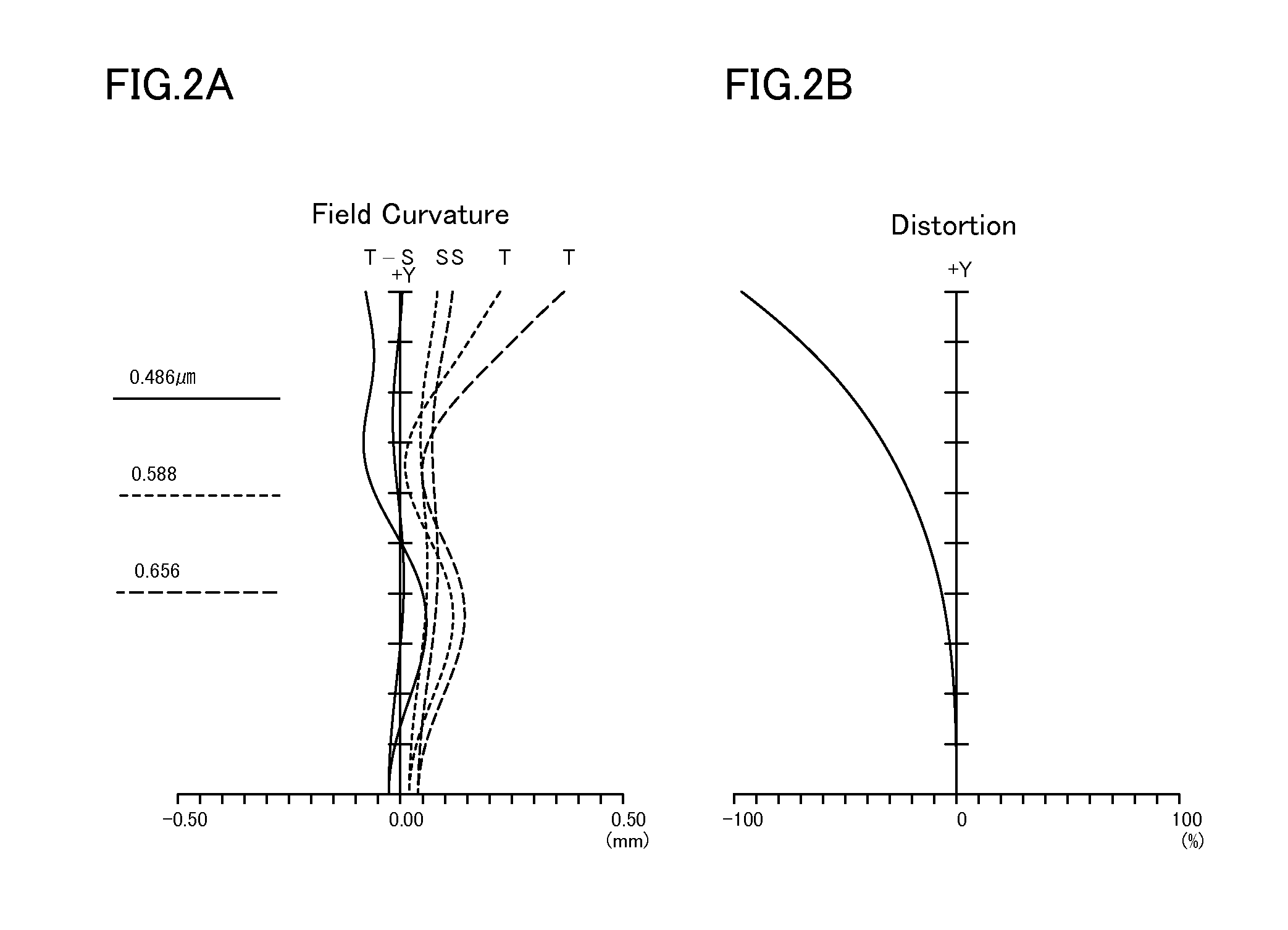
[0077]Hereinafter, there will be explained Example 1 in which the imaging optical system 100 shown in FIG. 1 is numerically defined. The following Table 1 shows lens data of the imaging optical system 100 in Example 1. Meanwhile, FIG. 1 also shows the lenses in Example 1.

TABLE 1s-nRdndν 119.86960.751.5163364.07 23.51352.2516 3*−38.2660.651.4874970.24 4*2.04412.0049 5*−31.20460.351.4966055.71 6*2.99150.4502 7*2.65610.921.5491734.65 8*2025.9860.6446 9*10.46290.651.4966055.7110*−3.39860.756311SInfinity012*2.58930.7351.4966055.7113*3.33550.919714*−5.7340.8051.4966055.7115*−1.1970.553316Infinity0.44271.5230858.5717Infinity0.8458aspherical coefficients-nc-c4th6th8th10th399.21668.7635E−05−1.1277E−05−1.2761E−062.1479E−084−0.7563.7427E−04−2.9575E−04−4.2577E−05−1.7225E−06570.6001−1.4871E−03−1.3311E−03−1.9180E−04−8.8441E−056−0.5776−1.8238E−035.4686E−04−7.8234E−04−3.2071E−0470.21353.2228E−041.8606E−043.8017E−04−1.1788E−058100.33262.0149E−036.2383E−04−3.0196E−043.7798E−04916.9326−1.9480E−03−1.50...

second embodiment

[0083]Hereinafter, an imaging optical system according to a second embodiment will be explained. Meanwhile, the imaging optical system according to the second embodiment is a modification of the imaging optical system of the first embodiment and the part which is not explained in particular is the same as the part in the first embodiment.

[0084]As shown in FIG. 3, the imaging optical system 100 of the present embodiment is constituted of seven lenses 10 to 70 and the lens number j is a number from 1 to 7. Furthermore, any of the lenses 10 to 70 is a single lens, the respective single lenses constitute each of lens groups, and the lens group number i coincides with the lens number j. Moreover, the aperture stop ST indicating the aperture stop position is located between the fifth lens 50 having a lens number 5 and the sixth lens 60 having a lens number 6, and m is 5.

[0085]In the imaging optical system 100 shown in FIG. 3, the lenses 20 to 70 except the lens 10 are aspherical lenses. I...


PUM


Abstract

There are provided an imaging optical system and imaging equipment, which are compatible with a solid-state imaging device having a size of ½ inches or less and which include an optical system having a small size and lightness in weight and also having an excellent mass productivity and a low cost while keeping optical performance at a wide field angle, for example, at a total angle of view of 80 degrees or more. When predetermined conditions are satisfied for a plurality of lenses constituting the imaging optical system, the absolute value of power of each lens group is suppressed to be small, and thus the generation of aberration is suppressed and a preferable aberration is obtained.

Description

INCORPORATION BY REFERENCE TO ANY PRIORITY APPLICATIONS[0001]Any and all applications for which a foreign or domestic priority claim is identified in the Application Data Sheet as filed with the present application are hereby incorporated by reference under 37 CFR 1.57.CROSS-REFERENCE TO RELATED APPLICATIONS[0002]This application claims the benefit of priority to Japanese Patent Application No. 2013-070294, entitled “Imaging Optical System and Imaging Equipment” filed on Mar. 28, 2013. The disclosure of the above-described application is hereby expressly incorporated by reference in its entirety.BACKGROUND[0003]1. Field of the Invention[0004]The present invention relates to an imaging optical system for imaging equipment and imaging equipment each of which uses a compact solid-state imaging device such as a CCD image sensor and a CMOS image sensor having a size of ½ inches or less.[0005]2. Description of the Related Art[0006]In imaging equipment using the solid-state imaging device,...

Claims


Application Information

Patent Timeline
IPC IPC(8): G02B3/04H04N5/351
CPCH04N5/351G02B3/04G02B13/0045G02B13/04G02B13/0085G02B13/18H04N25/50
Inventor SASAYA, TOSHIHIRO
Owner SASAYA TOSHIHIRO
Learn More