Microelectronic Displacement Damage Dose Detector

a technology of microelectronic displacement and detector, applied in the direction of optical radiation measurement, photometry using electric radiation detector, instruments, etc., can solve the problems of increasing risk, increasing radiation exposure, and reducing the service life of standard integrated circuits

Active Publication Date: 2014-10-23
UNITED STATES OF AMERICA
View PDF1 Cites 9 Cited by
  • Summary
  • Abstract
  • Description
  • Claims
  • Application Information

AI Technical Summary

Benefits of technology

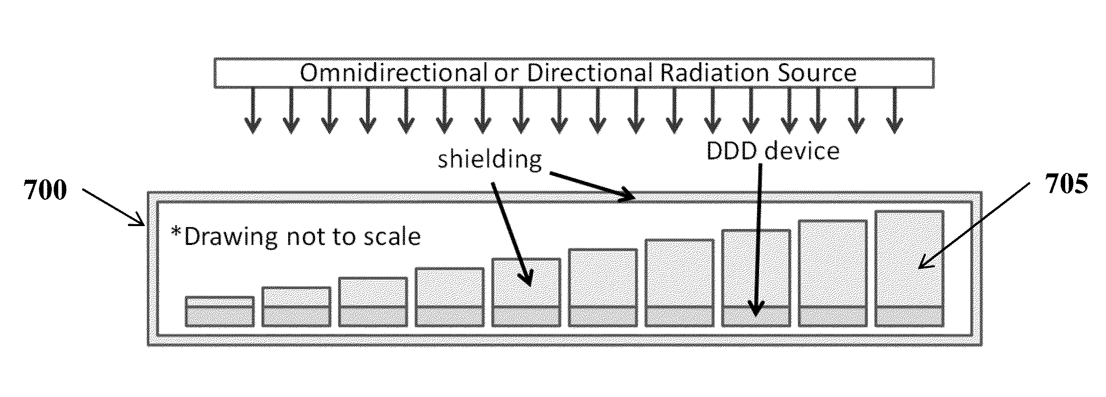
[0012]According to one aspect of the invention, a device is described that includes sensors that are sensitive to displacement damage, and can be configured to display a characteristic damage curve. The sensors, or diodes, can be made of one or more semiconductor materials that are sensitive to displacement damage, and can be operated in dark illumination conditions. The sensors can have multiple shields of a specific or varied thickness. The shields can be formed in different configurations, though the shielding thickness can be designed to change...

Problems solved by technology

This exposure to radiation has always been an issue for satellites.
Standard integrated circuits can gradually degrade or even catastrophically fail when exposed to the space radiation environment thereby necessitating special radiation-hardened components for satellites.
Radiation remains one of the leading causes of satellite anomalies; and as technology advances, the risk increases.
1. Single Event Effects (SEE): Single interactions, either large ionization or a nuclear reaction, that can give temporary or permanent damage to a given detector or system. SEE effects are important for digital circuits such as memories or microprocessor by inducing errors, undesired latch-ups and may lead to system failure.
2. Total Ionization Dose (TID): Effects caused by long-term exposure to ionizing radiation. TID may induce changes in the mechanical and electrical properties of materials, causing them to operate incorrectly or even fail. TID effects are important for insulators, cabling, CMOS circuits (due to charge build-up), optical ...

Method used


Image

  • Microelectronic Displacement Damage Dose Detector
  • Microelectronic Displacement Damage Dose Detector
  • Microelectronic Displacement Damage Dose Detector

Examples


Embodiment Construction

[0026]One or more embodiments or implementations are hereinafter described in conjunction with the drawings, where like reference numerals refer to like elements throughout, and where the various features are not necessarily drawn to scale.

[0027]Similarly, to the JPL model discussed above, the Naval Research Laboratory (NRL) developed a technique to predict on-orbit performance based on displacement damage dose with the results comparing well to the JPL model. The NRL model demonstrated that, using the calculated nonionizing energy loss (NIEL) to correlate displacement damage radiation effects due to different energetic particles, ground-based radiation data can be reduced to two, characteristic radiation degradation, or damage, curves. One of the curves can be for proton and neutron damage, and the other one can be for equivalent 1 MeV electrons. The NRL model implied that the characteristic curves could be obtained using much less ground testing; thereby saving significant time an...


PUM


Abstract

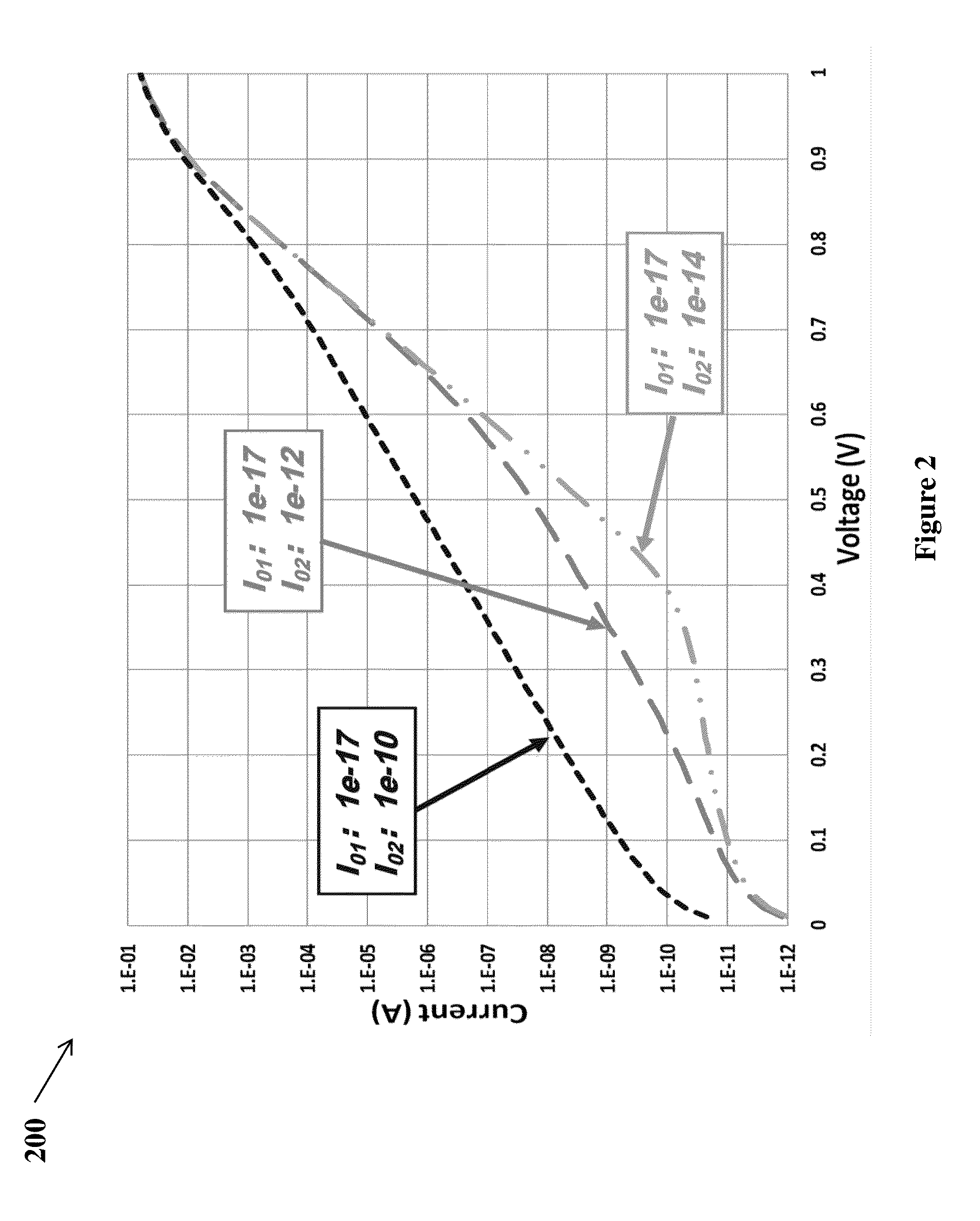
A device is described that includes sensors that are sensitive to displacement damage, and can be configured to display a characteristic damage curve. The sensors, or diodes, can be made of one or more semiconductor materials that are sensitive to displacement damage, and can be operated in dark illumination conditions. The sensors can have multiple shields of a specific or varied thickness. The shields can be formed in different configurations, though the shielding thickness can be designed to change the level of displacement damage absorbed by the sensors. The characteristic damage curve can provide a sensor response variable that displays a functional dependence on displacement damage. For example, the characteristic damage curve can provide a sensor response variable that is one or more currents measured at one or more fixed voltages, or one or more voltages measured at one or more fixed currents.

Description

CROSS-REFERENCE TO RELATED APPLICATIONS[0001]This application claims priority to provisional patent application entitled, “A MICROELECTRONIC DISPLACEMENT DAMAGE DOSE DETECTOR,” filed on Mar. 11, 2013, and assigned U.S. Application No. 61 / 775,914; and to provisional patent application entitled “AN ELECTRONIC DISPLACEMENT DAMAGE DOSE DETECTOR,” filed on Mar. 15, 2013, and assigned U.S. Application No. 61 / 786,700. The entire contents of both applications are hereby incorporated by reference.FIELD OF THE INVENTION[0002]The present disclosure relates generally to measuring the effects of radiation on components, such as spacecraft components. More specifically, it relates to a microelectronic device that can be used to accurately and simply quantify displacement damage dose directly, with applications in both ground-based and space-based radiation environment displacement damage dosimetry.BACKGROUND[0003]A satellite flying in Earth orbit is subjected to a particle (electron and proton) r...

Claims


Application Information

Patent Timeline
IPC IPC(8): G01T1/02G01D9/00
CPCG01D9/005G01T1/026
Inventor MESSENGER, SCOTT R.CRESS, CORY D.YAKES, MICHAEL K.WARNER, JEFFREY H.WALTERS, ROBERT J.
Owner UNITED STATES OF AMERICA
Why Eureka
Try Eureka