El display device and method for producing same

a technology of display device and light-emitting layer, which is applied in the direction of electroluminescent light source, thermoelectric device, electric lighting source, etc., can solve the problems of high precision sputtering and difficulty in patterning these layers, and achieve the effect of suppressing material deterioration, low barrier of easy injection into light-emitting layer

Inactive Publication Date: 2014-10-23
JOLED INC
View PDF3 Cites 14 Cited by
  • Summary
  • Abstract
  • Description
  • Claims
  • Application Information

AI Technical Summary

Benefits of technology

[0010]In the EL display device pertaining to one embodiment of the present invention, the material deterioration suppressing layer containing barium as a major component is formed on the light-emitting layer, and thus a material for the light-emitting layer is less likely to deteriorate. This is because the material deterioration suppressing layer containing barium as a major component has a low electron level. Therefore, a barrier of injection into the light-emitting layer is low, and electrons are easily injected into the light-emitting layer. Further, the material deterioration suppressing layer contains therein large quantities of free electrons. Therefore, when such a layer is formed on the light-emitting layer, charges accumulated in the light-emitting layer are allowed to escape into the material deterioration suppressing layer. Accordingly, charges are less likely to accumulate in the light-emitting layer, and a material for the light-emitting layer hardly deteriorates. The material deterioration suppressing layer can suppress deterioration of a material for the light-emitting layer even if it is extremely thin. The effect of suppressing the deterioration, however, increases with increasing thickness of the material deterioration suppressing layer.
[0011]Furthermore, since the thickness of the material deterioration suppressing layer is 10 nm or smaller, even when the material deterioration suppressing layer and the transition metal oxide layer are each formed as a solid film, a wiring portion that is the portion of the material deterioration suppressing layer above the auxiliary wiring does not serve as an insulating film, and passage of current between the auxiliary wiring and the common electrode is less likely to be prevented. That is to say, when the material deterioration suppressing layer and the transition metal oxide layer are each formed as a solid film, these layers can be in contact with each other above the auxiliary wiring. In such a case, barium in the wiring portion of the material deterioration suppressing layer is oxidized to barium oxide upon receiving oxygen supply from the transition metal oxide layer, and the wiring portion becomes highly resistive. If the thickness of the material deterioration suppressing layer is 10 nm or greater in this case, the highly-resistive wiring portion serves as an insulating film, and thus passage of current between the auxiliary wiring and the common electrode is prevented. On the other hand, when the thickness of the material deterioration suppressing layer is smaller than 10 nm, passage of current is ensured by tunnel current even if the wiring portion becomes highly resistive.
[0012]The method for manufacturing the EL display device pertaining to one embodiment of the present invention includes a step of forming the material deterioration suppressing layer as described above. Thus, by using the method for manufacturing the EL display device pertaining to one embodiment of the present invention, an EL display device whose life is less likely to be reduced by deterioration of a material for the light-emitting layer can be manufactured. In addition, since the transition metal oxide layer is formed continuously on the pixel electrode and on the auxiliary wiring, and the material deterioration suppressing layer is formed continuously on the portion of the transition metal oxide layer above the auxiliary wiring and on the light-emitting layer, a manufacturing process can be simplified.

Problems solved by technology

Further, the pixel electrode, which is formed for each pixel, and the hole transport layer and the organic light-emitting layer, which are formed by printing, are patterned, whereas the hole injection layer, the electron transport layer, and the common electrode are formed as a continuous film, or a so-called “solid film”, without being patterned, as there is no need to form these layers for each pixel, and it is not easy to pattern these layers formed by evaporation and sputtering with high precision.

Method used


Image

  • El display device and method for producing same
  • El display device and method for producing same
  • El display device and method for producing same

Examples


experiment 1

[0075](Experiment 1) Effect of Material Deterioration Suppressing Layer on Deterioration of Material for Light-emitting Layer

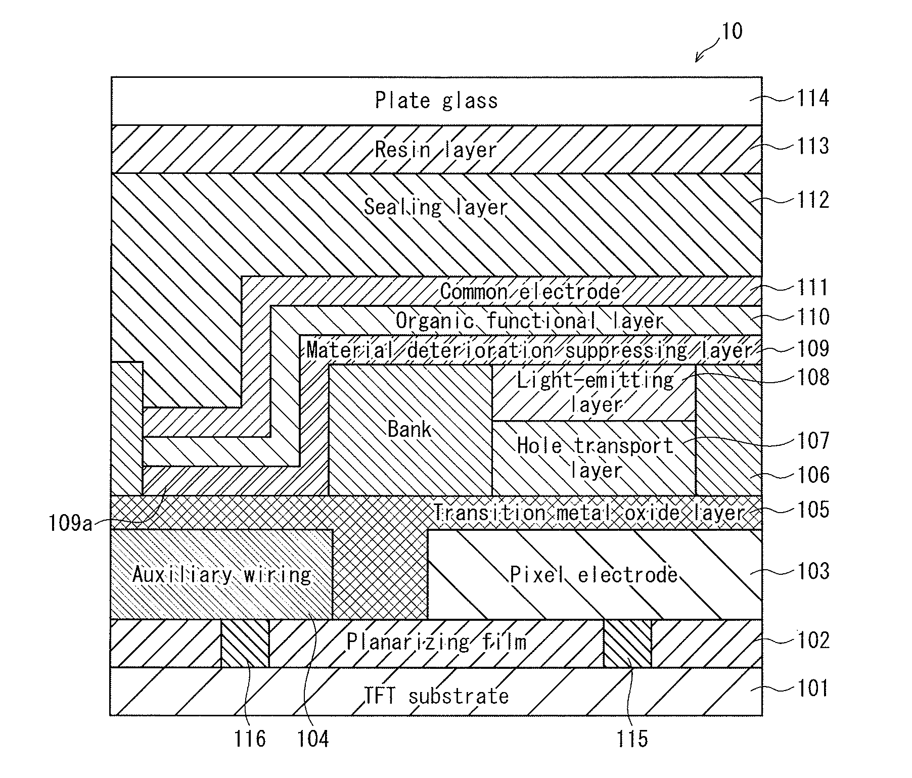
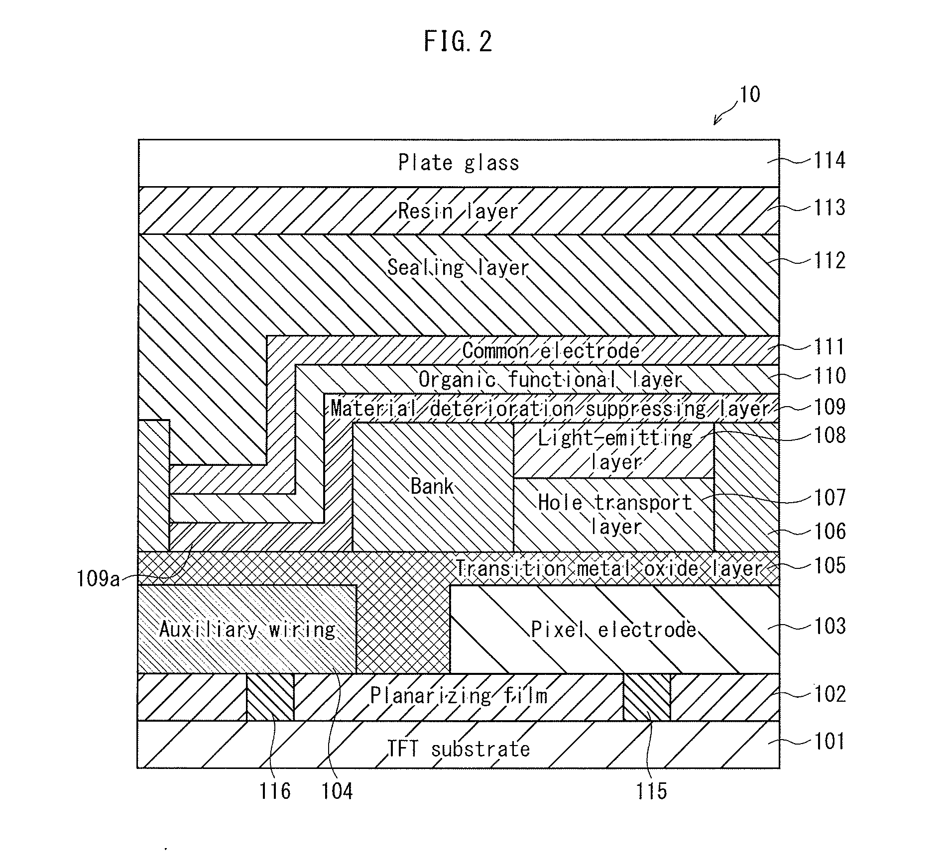
[0076]A reduced life of an organic EL display device is caused by a decrease in brightness, that is, a decrease in light-emitting efficiency (external quantum efficiency). One of the major factors of the decrease in light-emitting efficiency is deterioration of a material for the light-emitting layer. A degree of the deterioration of the material for the light-emitting layer can be evaluated based on internal quantum efficiency of the light-emitting layer. The internal quantum efficiency can quantitatively be known by measuring PL intensity. In order to examine the effect of the material deterioration suppressing layer on the deterioration of the material for the light-emitting layer, the inventors prepared an EL display device not including a material deterioration suppressing layer, an EL display device including a material deterioration suppressing layer ha...

experiment 2

[0080](Experiment 2) Insulating Properties of Wiring Portion of Material Deterioration Suppressing Layer

[0081]Next, in order to confirm the effect of the thickness of the material deterioration suppressing layer on the insulating properties of the wiring portion of the material deterioration suppressing layer, the inventors prepared devices each including a short circuit in which a hole transport layer, a light-emitting layer, and a bank are not formed, and checked conductivity between auxiliary wiring and the common electrode of each of the devices. Specifically, each of the devices includes a planarizing film, a pixel electrode, the auxiliary wiring, a transition metal oxide layer, a material deterioration suppressing layer, an organic functional layer, and the common electrode stacked on a TFT substrate.

[0082]FIG. 5 shows the effect of the thickness of the material deterioration suppressing layer on the insulating properties of the wiring portion. In FIG. 5, “Ref”, “Ba monolayer”...

experiment 3

[0084](Experiment 3) Lifetime Properties of EL Display Device

[0085]In order to confirm the effect of the thickness of the material deterioration suppressing layer on lifetime properties of the EL display device, EL display devices that were similar to those used in Experiment 1 were used to evaluate lifetime properties of these EL display devices.

[0086]FIG. 6 shows the effect of the thickness of the material deterioration suppressing layer on lifetime properties of the EL display device. In FIG. 6, relative brightness on the Y-axis is similar to that in Experiment 1. “Ba monolayer 0 nm”, “Ba monolayer 5 nm”, “Ba monolayer 10 nm” in FIG. 6 are also similar to those in Experiment 1.

[0087]As a result of driving the EL display devices over time while putting the same current load thereon, and measuring brightness of each of the EL display devices, the time until brightness was halved (time until relative brightness became 50%) was approximately 20 hours in the case where the material de...


PUM

PropertyMeasurementUnit
thicknessaaaaaaaaaa
thicknessaaaaaaaaaa
thicknessaaaaaaaaaa

Abstract

To provide a device whose life is less likely to be reduced by deterioration of a light-emitting layer material, an EL display device includes: a pixel electrode, for each pixel, above a substrate; auxiliary wiring in a different region, above the substrate, from the pixel electrode; a transition metal oxide layer on the pixel electrode and the auxiliary wiring; a light-emitting layer in a region, above the transition metal oxide layer, corresponding to the pixel; a common electrode continuously above the auxiliary wiring and the light-emitting layer, and electrically connected to the auxiliary wiring; and a material deterioration suppressing layer continuously on a portion of the transition metal oxide layer above the auxiliary wiring and the light-emitting layer, mainly containing barium, and having a thickness equal to or greater than a size of a single barium atom and smaller than 10 nm.

Description

TECHNICAL FIELD [0001]The present invention relates to EL display devices and methods for manufacturing the same, and, in particular, to technology for improving lifetime properties of EL display devices.BACKGROUND ART[0002]One example of EL display devices is an organic EL display device making use of electro-luminescence in organic materials. A top-emission type organic EL display device includes, for example, a pixel electrode formed on a substrate, and a hole injection layer, a hole transport layer, an organic light-emitting layer, an electron transport layer, and a common electrode stacked on the pixel electrode. In the organic EL display device having such a structure, in order to prevent voltage drop produced in the common electrode with increasing size of a screen of the device, auxiliary wiring electrically connected to the common electrode is formed in a region, above the substrate, in which the pixel electrode is not formed (Patent Literature 1).[0003]In a process of form...

Claims


Application Information

Patent Timeline
Patent Type & Authority Applications(United States)
IPC IPC(8): H01L51/50H01L51/56
CPCH01L51/5088H01L51/56H01L51/5012H05B33/10H10K59/123H10K59/1315H10K50/814H10K50/826H10K50/844H10K50/17H10K50/11H10K50/166H10K71/00
Inventor ISOBE, TAKASHI
Owner JOLED INC
Why Eureka
Try Eureka