Process for smoothing a surface via heat treatment

a heat treatment and surface technology, applied in the field of smoothing process, can solve the problems of large roughness, incompatibility with the targeted application, and requires a relatively long implementation time for very rough surfaces, so as to reduce the roughness of the surface, avoid the use of dangerous gases, and facilitate the effect of implementation

Active Publication Date: 2014-10-23
COMMISSARIAT A LENERGIE ATOMIQUE ET AUX ENERGIES ALTERNATIVES
View PDF1 Cites 4 Cited by
  • Summary
  • Abstract
  • Description
  • Claims
  • Application Information

AI Technical Summary

Benefits of technology

The patent text describes a method for smoothing the surface of a semiconductor alloy substrate made from at least two elements chosen from Ga, As, Al, In, P, and N. The method involves placing a second substrate facing the rough surface of the first substrate, with a distance between them of at least 10 μm. The first substrate is then heated to partially desorb one of the alloy elements and create a confinement space between the two substrates. This results in a surface atom mobility that reduces the roughness of the rough surface. The technical effect of this method is that it provides a simple, inexpensive, and safe way to smooth the surface of semiconductor alloy substrates.

Problems solved by technology

The dicing process produces substrates having rough surfaces and comprising structural defects such as dislocations in the crystal lattice.
The surfaces obtained after splitting, in particular in the case of transfer of thin layers of gallium and arsenic alloy (GaAs) or of indium and phosphorus alloy (InP) present a large roughness, incompatible with the targeted application.
This solution is however onerous and requires a relatively long implementation time for very rough surfaces.
Transposition of this thermal smoothing technique to semiconductor alloy substrates, for example made from GaAs or from InP, does however remain difficult to achieve.
Indeed, when heat treatment is performed at high temperatures, typically above 500° C. for GaAs and InP, these semiconductor alloys can decompose.
However, this type of heat treatment requires handling of dangerous gases such as arsine (AsH3) and means that a costly specific installation has to be set up.
Furthermore, scratches may appear on the surfaces as the surfaces remain in contact after splitting.

Method used


Image

  • Process for smoothing a surface via heat treatment
  • Process for smoothing a surface via heat treatment
  • Process for smoothing a surface via heat treatment

Examples


Embodiment Construction

[0015]A dependable, practical and inexpensive means for producing substrates comprising a semiconductor alloy based on at least two elements chosen from Ga, As, Al, In, P and N having at least one smooth surface devoid of structural defects consists in using smoothing by heat treatment with standard equipment and atmospheres by locally creating an atmosphere preventing a great decomposition of this alloy, at the level of the surface to be treated.

[0016]For activation of dopants or to improve the electric properties of substrates made from semiconductor alloys, for example from GaAs or InP, it has already been proposed to perform heat treatment by placing two substrates on top of one another. This solution, called proximity cap, enables the decomposition phenomenon of substrates made from semiconductor alloys to be limited when these specific heat treatments are performed.

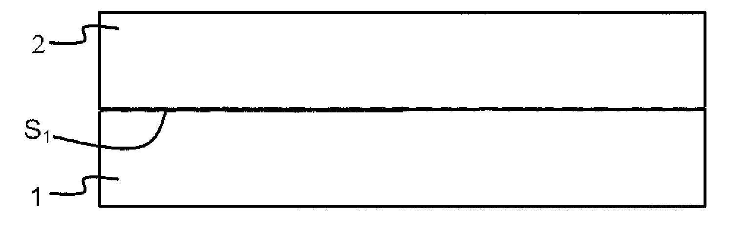
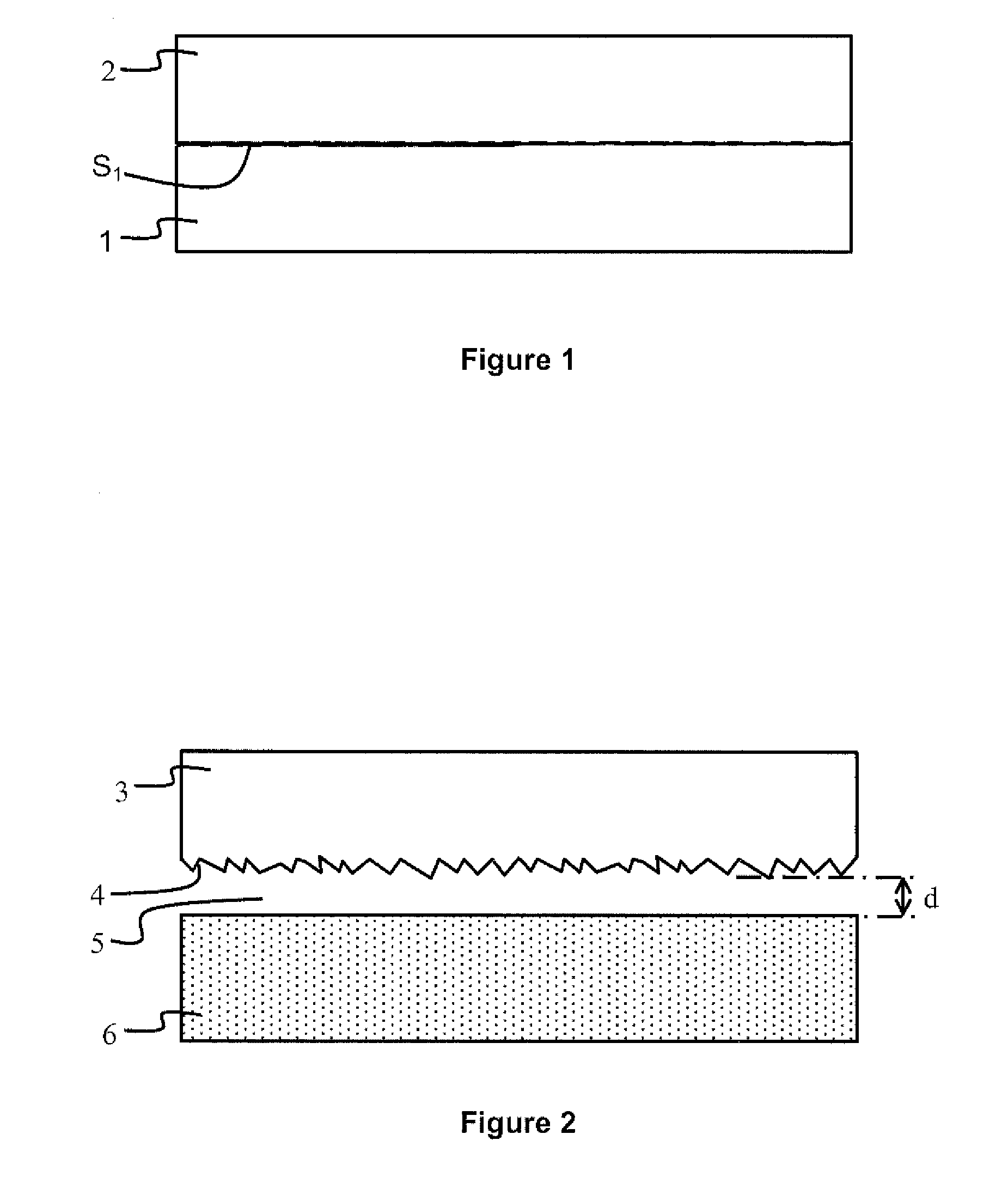
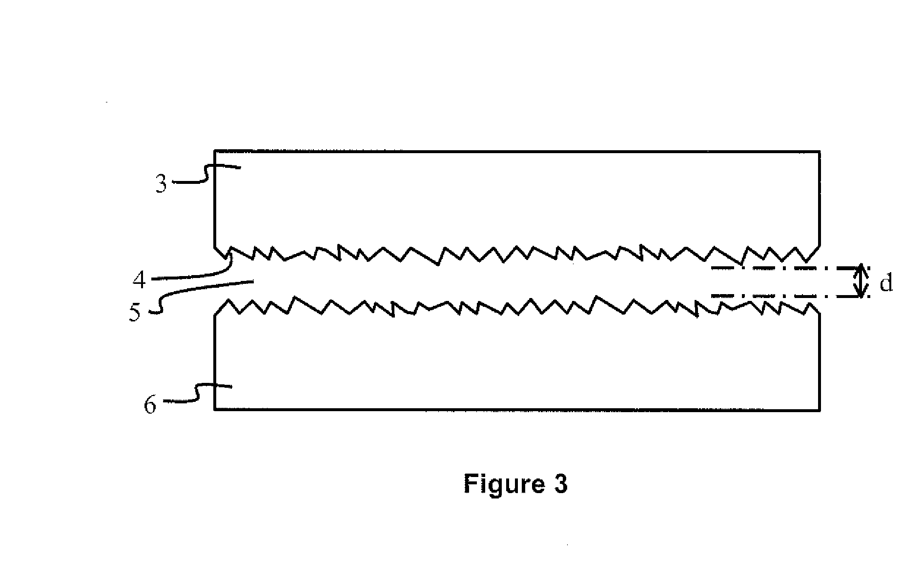
[0017]As represented in FIG. 1, the proximity method consists in placing a protection substrate 2 on the useful s...


PUM


Abstract

The process for smoothing a rough surface of a first substrate made of a semiconductor alloy based on at least two elements chosen from Ga, As, Al, In, P and N is implemented by placing a second substrate facing the first substrate so that the rough surface is placed facing a surface of the second substrate. The first and second substrates are separated by a distance d of at least 10 μm, the facing portions of the two substrates defining a confinement space. The first substrate is then heated so as to partially desorb one of the elements of said alloy and to reach the saturated vapor pressure of this element in the confinement space and to obtain a surface atom mobility that is sufficient to reduce the roughness of the rough surface.

Description

BACKGROUND OF THE INVENTION[0001]The invention relates to a smoothing process, using heat treatment, of a rough surface of a first substrate comprising at the surface a semiconductor alloy based on at least two elements chosen from Ga, As, Al, In, P and N.STATE OF THE ART[0002]Substrates made from semiconductor material are generally obtained by dicing an ingot made from the same semiconductor material. The dicing process produces substrates having rough surfaces and comprising structural defects such as dislocations in the crystal lattice. A technique also exists involving transfer of thin films of semiconductor material, known under the name of Smart Cut™. This technique in general comprises three steps: a first step of ion implantation of hydrogen and / or of rare gases to create a weakened buried layer in the initial substrate, a second step of securing the initial substrate with a receiver substrate (or strengthener), and a third step of heat treatment to obtain a split off at th...

Claims


Application Information

Patent Timeline
IPC IPC(8): H01L21/324H01L21/302
CPCH01L21/302H01L21/3247H01L21/3245H01L21/76254H01L21/26506
Inventor JOUANNEAU, THOMASBOGUMILOWICZ, YANN
Owner COMMISSARIAT A LENERGIE ATOMIQUE ET AUX ENERGIES ALTERNATIVES
Why Eureka
Try Eureka