On-device metrology

a metrology and device technology, applied in the field of metalrology systems and methods, can solve the problems of difficult optical radiation penetration to the bottom layer, difficult characterization, and more difficult characterization, and achieve the effect of eliminating or improving accuracy of measurements

Active Publication Date: 2014-10-23
KLA TENCOR TECH CORP
View PDF0 Cites 133 Cited by
  • Summary
  • Abstract
  • Description
  • Claims
  • Application Information

AI Technical Summary

Benefits of technology

[0015]In one further aspect, measurement data from both on-device measurement targets and assist targets that may be found on-device or within scribe lines is collected for model building, training, and measurement. In some examples, the use of measurement data associated with multiple targets eliminates, or significantly reduces, the effect of under layers in the measurement result. The use of measurement data associated with multiple targets increases the sample and process information embedded in the model. In particular, the use of training data that includes measurements of multiple, different targets at one or more measurement sites enables more accurate measurements.

Problems solved by technology

As devices (e.g., logic and memory devices) move toward smaller nanometer-scale dimensions, characterization becomes more difficult.
Devices incorporating complex three-dimensional geometry and materials with diverse physical properties contribute to characterization difficulty.
For example, modern memory structures are often high-aspect ratio, three-dimensional structures that make it difficult for optical radiation to penetrate to the bottom layers.
As a result, the measurement model parameters characterizing the target often cannot be reliably decoupled.
In response to these challenges, more complex optical tools have been developed.
In addition, the spreading of light intensity over large wavelength ranges decreases illumination intensity at any particular wavelength and increases signal uncertainty of measurements performed at that wavelength.
Each step introduces errors and consumes a significant amount of computational and user time.
Typically, a model building task requires days, or even weeks, to complete.
In addition, the size of the library and the computation time associated with performing regression calculations during measurement reduces the throughput of the measurement system.
The use of dedicated metrology structures may introduce significant measurement errors.
Discrepancies between actual device structures and dedicated metrology targets limit the ability of metrology data to accurately reflect the status of the actual device features in the die.
In one example, discrepancies arise due to location dependent differences in process loading, pattern density, or aberration fields because the dedicated metrology targets and actual device structures are not collocated.
Hence, even if the dedicated metrology target and the actual device structure are in close proximity, discrepancies result from differences in size.
Furthermore, dedicated metrology structures require space in the device layout.
Future metrology applications present challenges for metrology due to increasingly small resolution requirements, multi-parameter correlation, increasingly complex geometric structures, and increasing use of opaque materials.

Method used


Image

  • On-device metrology
  • On-device metrology
  • On-device metrology

Examples


Embodiment Construction

[0036]Reference will now be made in detail to background examples and some embodiments of the invention, examples of which are illustrated in the accompanying drawings.

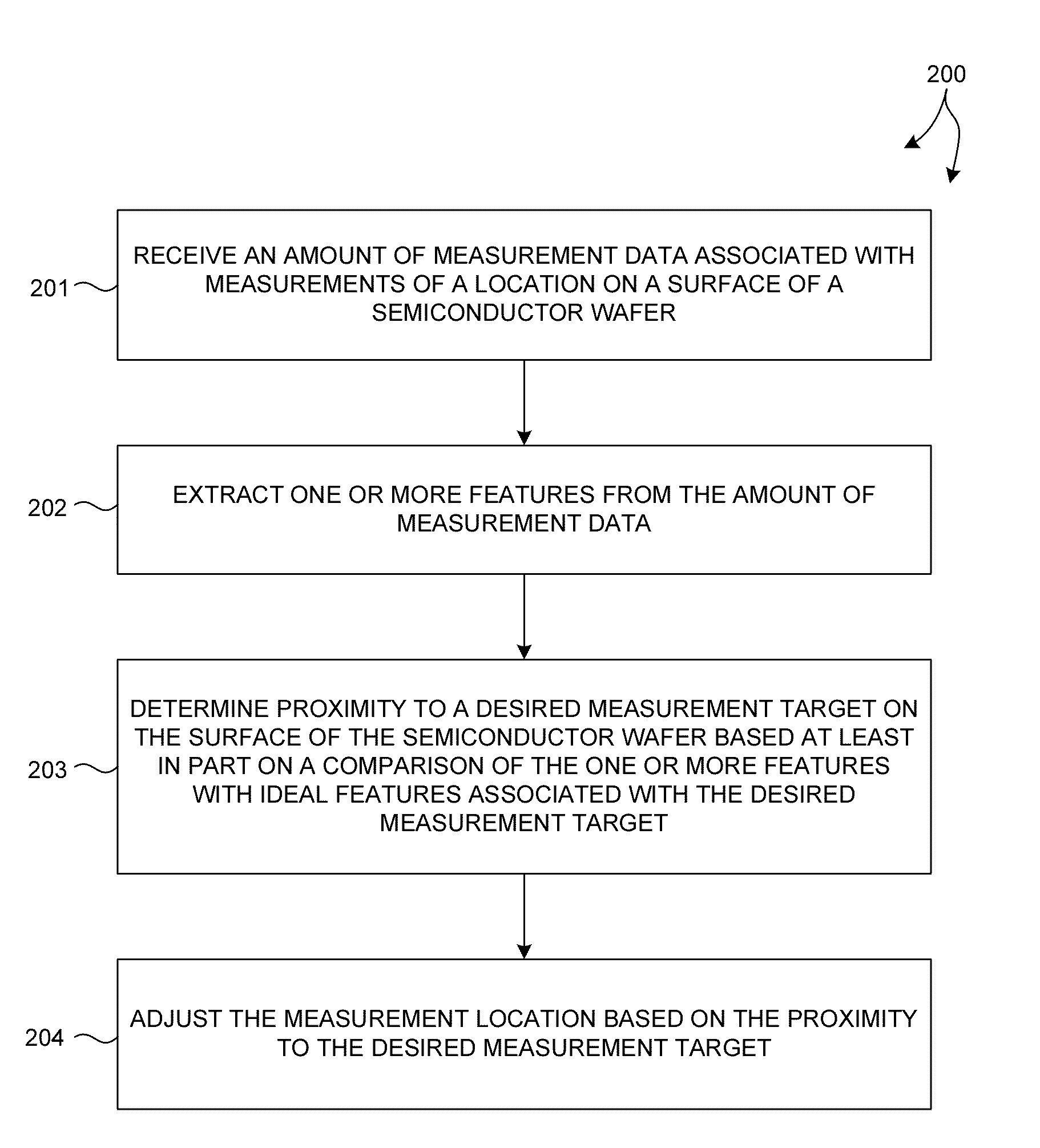
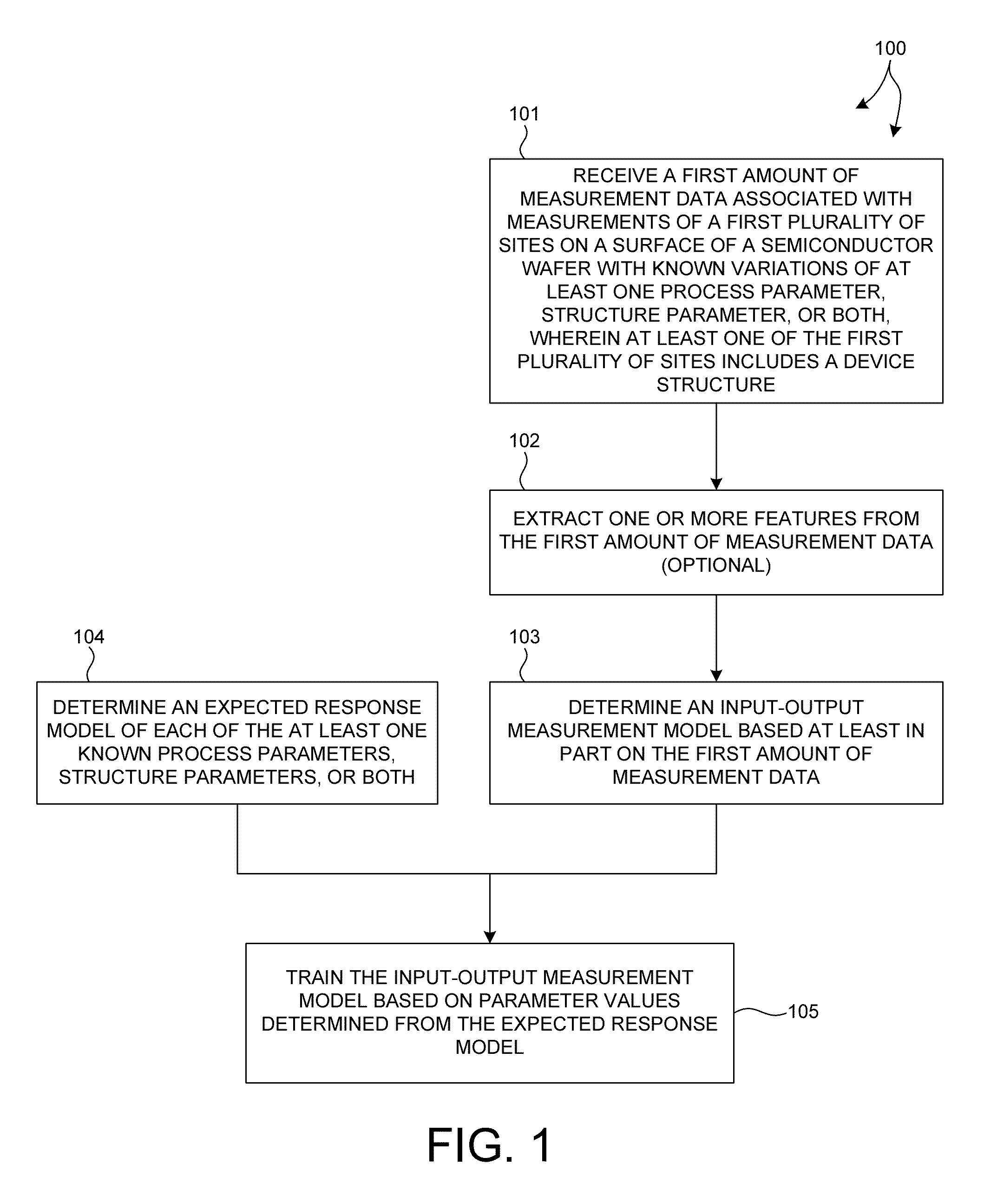
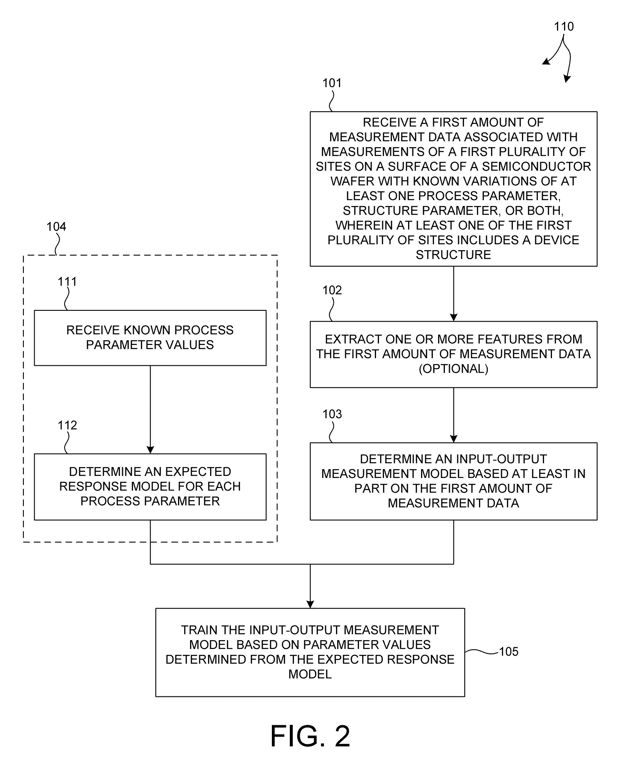
[0037]Methods and systems for performing semiconductor metrology directly on the actual device structure are presented.

[0038]In one aspect, a measurement model is created based only on measured training data (e.g., spectra collected from a Design of Experiments (DOE) wafer) collected from at least one actual device structure. The trained measurement model is then used to calculate process parameter values, structure parameter values, or both, directly from measured data (e.g., spectra) collected from actual device structures of other wafers. In this manner, only spectra acquired from samples is required to create a measurement model and to perform measurements using the model.

[0039]The measurement models described herein receive measurement data (e.g., measured spectra) directly as input and provide process parameter ...


PUM


Abstract

Methods and systems for performing semiconductor metrology directly on device structures are presented. A measurement model is created based on measured training data collected from at least one device structure. The trained measurement model is used to calculate process parameter values, structure parameter values, or both, directly from measurement data collected from device structures of other wafers. In some examples, measurement data from multiple targets is collected for model building, training, and measurement. In some examples, the use of measurement data associated with multiple targets eliminates, or significantly reduces, the effect of under layers in the measurement result, and enables more accurate measurements. Measurement data collected for model building, training, and measurement may be derived from measurements performed by a combination of multiple, different measurement techniques.

Description

CROSS REFERENCE TO RELATED APPLICATION[0001]The present application for patent claims priority under 35 U.S.C. §119 from U.S. provisional patent application Ser. No. 61 / 814,191, entitled “On-Device Metrology,” filed Apr. 19, 2013, the subject matter of which is incorporated herein by reference in its entirety.TECHNICAL FIELD[0002]The described embodiments relate to metrology systems and methods, and more particularly to methods and systems for improved parameter measurement.BACKGROUND INFORMATION[0003]Semiconductor devices such as logic and memory devices are typically fabricated by a sequence of processing steps applied to a specimen. The various features and multiple structural levels of the semiconductor devices are formed by these processing steps. For example, lithography among others is one semiconductor fabrication process that involves generating a pattern on a semiconductor wafer. Additional examples of semiconductor fabrication processes include, but are not limited to, ch...

Claims


Application Information

Patent Timeline
Patent Type & Authority Applications(United States)
IPC IPC(8): H01L21/66
CPCH01L22/12H01L22/34H01L2924/0002H01L22/20H01L22/30H01L2924/00
Inventor SHCHEGROV, ANDREI V.MADSEN, JONATHAN M.PANDEV, STILIAN IVANOVLEVY, ADYKANDEL, DANIELADEL, MICHAEL E.TADMOR, ORI
Owner KLA TENCOR TECH CORP
Why Eureka
Try Eureka