Graphene-based nanodevices for terahertz electronics

Active Publication Date: 2014-10-30
UNIV AUGSBURG
View PDF13 Cites 21 Cited by
  • Summary
  • Abstract
  • Description
  • Claims
  • Application Information

AI Technical Summary

Benefits of technology

[0022]The operation principle of the proposed devices is based on the known physical effect that electrons, moving with an acceleration, radiate electromagnetic waves (Smith-Purcell effect, Ref.). In the proposed devices electrons move in the working area (active layer of graphene), under the action of an applied source-drain voltage, with a rather high velocity of order of v0≈108 cm / s. The working area (active layer) is a specially designed one-atom-thick layer (monolayer) of graphene. Above the graphene monolayer there exists a thin conducting grating, which also can be made out of a specially designed graphene monolayer. A small dc voltage (one to a few Volt) is applied between the grating and the active graphene layer. This voltage induces a periodic potential U(x)=U(x+ax) in the plane of the active graphene layer (here ax is the grating period along the longitudinal direction x), so that the moving electrons(vx≃v0, x≃v0·t) experience a periodic in time force Fx(t)=Fx(t+v0·t / ax). As a result, they get an oscillating contribution to their velocity,

Problems solved by technology

This bandwith is known as the terahertz gap, because it proved to be difficult to produce suitable and small devices emitting electromagnetic radiation in this frequency range with enough power.

Method used


Image

  • Graphene-based nanodevices for terahertz electronics
  • Graphene-based nanodevices for terahertz electronics
  • Graphene-based nanodevices for terahertz electronics

Examples


first embodiment

[0032]FIG. 8: the nanodevice according to the second aspect of the invention having a one-layer graphene structure with a modulated width of stripes in the transversal direction y.

second embodiment

[0033]FIG. 9: the nanodevice according to the second aspect of the invention having a one-layer graphene structure with an array of holes producing a modulation of the width of graphene stripes in the transversal direction y.

[0034]FIG. 10: Schematic illustration of a thin bended graphene-based nanodevice according to the invention focussing the emitted terahertz radiation to a focus of radiaton.

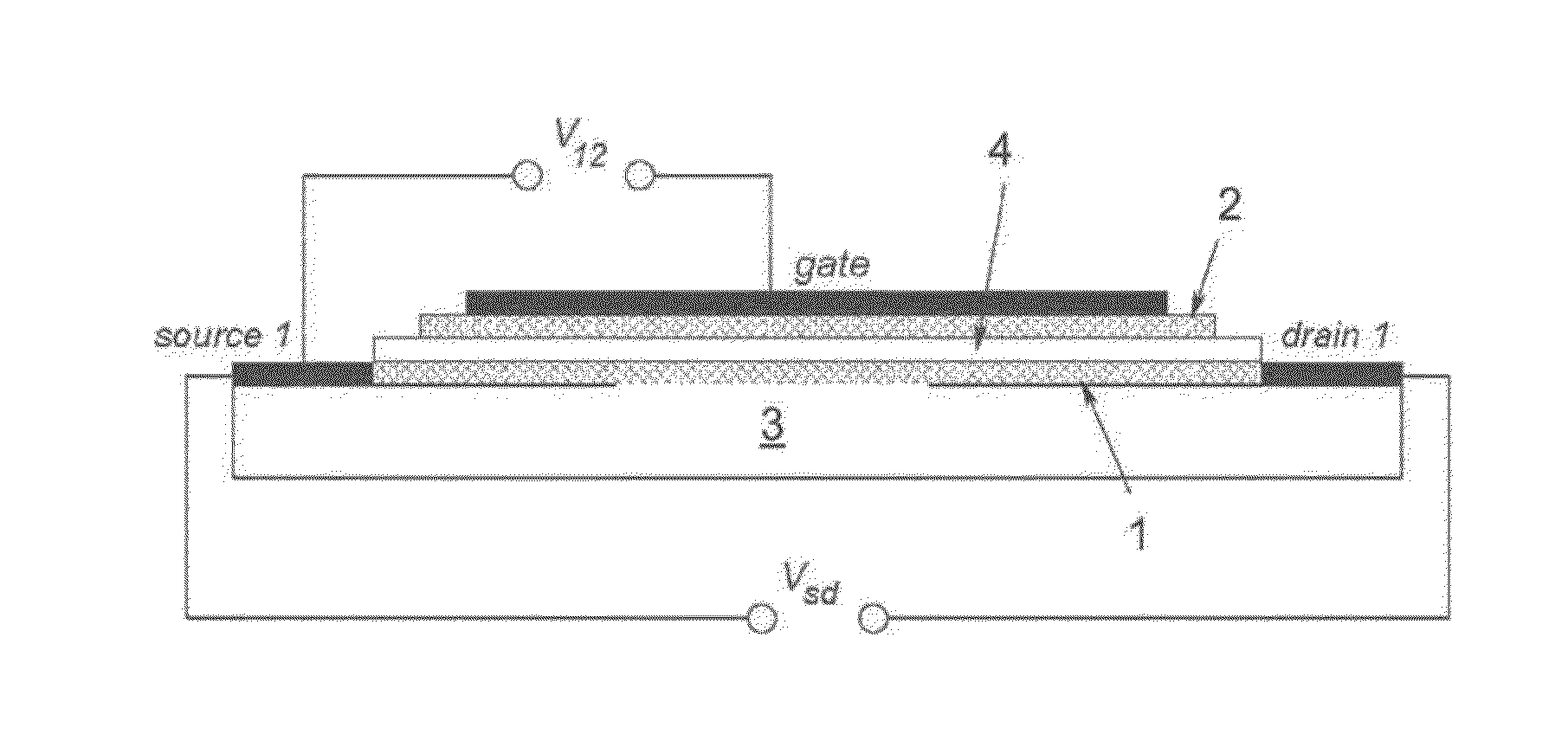
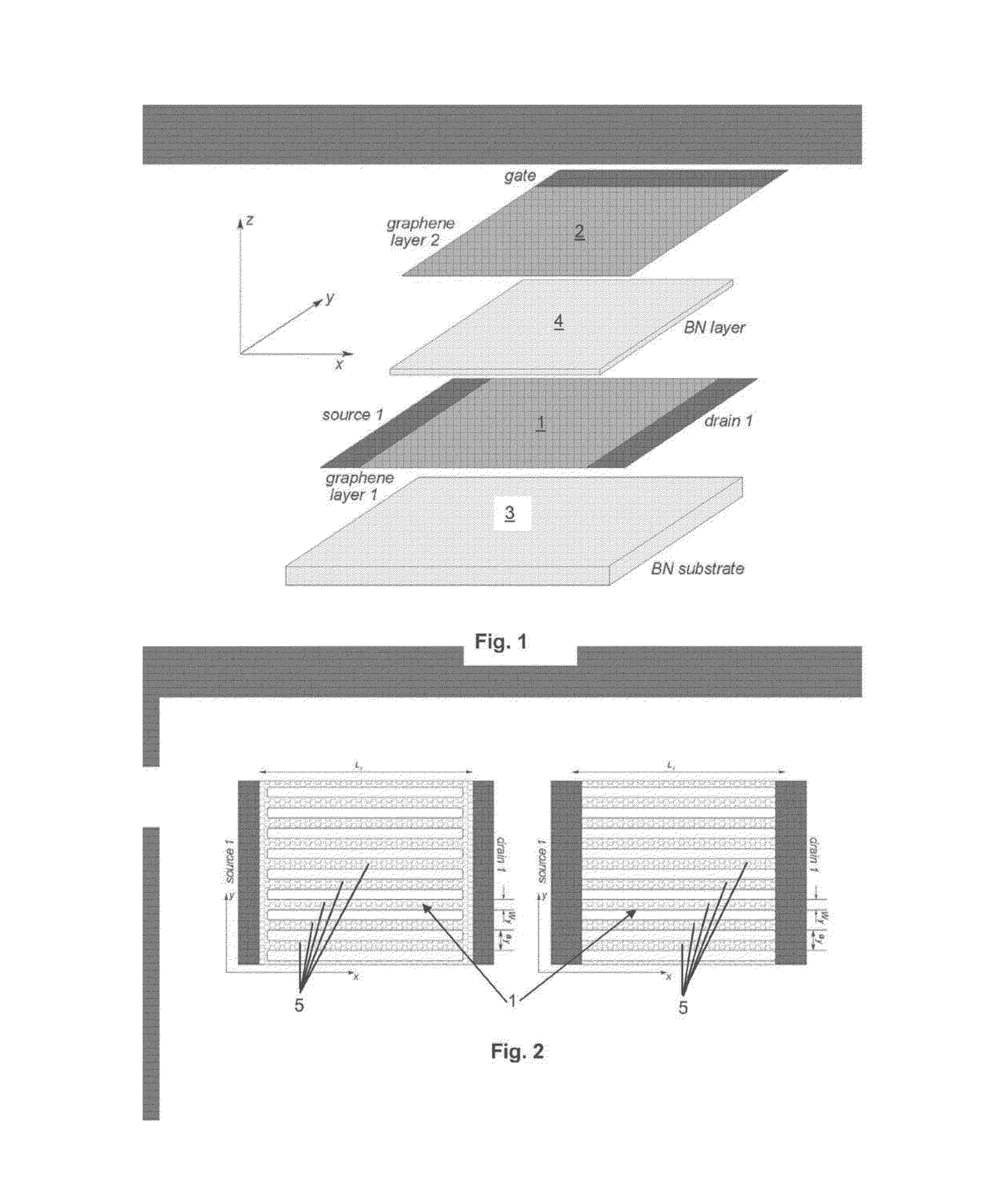
[0035]FIG. 1 shows a preferred embodiment of a basic design of the claimed nanodevice. The whole structure lies on a substrate 3 (marked as “BN substrate” in FIG. 1), which can be made out of any dielectric material, e.g. SiO2 or SiC, but the best one would be the hexagonal (graphitic) boron nitride (h-BN). On the substrate lies a first graphene layer marked as “graphene layer 1” in FIG. 1. This layer is structured as shown in FIG. 2 and has two longitudinal ends connected with metallic contacts “source1” and “drain1”, respectively. The first graphene layer 1 has the form of an array of narro...


PUM

PropertyMeasurementUnit
widthaaaaaaaaaa
grating periodaaaaaaaaaa
gate voltageaaaaaaaaaa

Abstract

The invention refers to a nanodevice for generating electromagnetic radiation in the terahertz frequency range, the nanodevice comprising a substrate (3) made of a dielectric material, a first graphene layer (1) arranged on the substrate (3), having a first longitudinal end being electrically connected with a source contact (source 1) and having a second longitudinal end being connected with a drain contact (drain 1), an electrically conducting layer (2) having a periodic grating structure with grating stripes (6) extending substantially in transversal direction (y), and a dielectric layer (4) arranged between the first graphene layer (1) and the conducting layer (2).

Description

TECHNICAL FIELD[0001]The invention refers to graphene-based nanodevices, namely a voltage tunable generator of electromagnetic radiation and a transistor (amplifier) combined with a plane antenna, operating at terahertz frequencies.BACKGROUND ART[0002]The terahertz frequency range is usually defined as 0.1 to 10 THz. Terahertz waves are electromagnetic waves with frequencies higher than microwaves but lower than infrared radiation and visible light. This bandwith is known as the terahertz gap, because it proved to be difficult to produce suitable and small devices emitting electromagnetic radiation in this frequency range with enough power. Terahertz waves possess many advantages for different applications, as for example in spectroscopy, non-destructive testing of non-conductive materials such as plastics, foam, composites, ceramics, paper, wood and glass, e.g. in space industry, non-ionizing medical imaging and tumor detection, high resolution close range radar and security detect...

Claims


Application Information

Patent Timeline
Patent Type & Authority Applications(United States)
IPC IPC(8): G21G4/06H01L29/16H01L33/00
CPCG21G4/06H01L29/1606H01L33/0041H01L29/4238H01L29/518H01L29/778H01L29/0657B82Y20/00G02F2203/13G02F2202/36
Inventor MIKHAILOV, SERGEY
Owner UNIV AUGSBURG
Why Eureka
Try Eureka