
Thin film transistor substrate and manufacturing method thereof

a technology of thin film transistors and substrates, applied in transistors, semiconductor devices, electrical equipment, etc., can solve the problems of low opening ratio and low transmittance of pixel display portions, difficult to achieve bright display characteristics, and liquid crystals on pixel electrodes not operating, etc., to suppress interface reaction and satisfy connection properties

Active Publication Date: 2014-10-30
TRIVALE TECH
View PDF24 Cites 16 Cited by
  • Summary
  • Abstract
  • Description
  • Claims
  • Application Information

AI Technical Summary

Benefits of technology

The present invention aims to improve the connection between a semiconductor layer and source / drain electrodes in a TFT substrate that includes a TFT using an oxide semiconductor for a semiconductor film and is driven by using a transverse electric field. The invention seeks to prevent film floating of an insulating film on a transparent conductive film and to suppress interface reaction between the semiconductor film and source and drain electrodes. The invention achieves this by increasing the contact area between the semiconductor film and the source / drain electrodes, reducing interface resistance and compensating for any failure in interface resistance on one surface of the semiconductor layer with successful compensation on the other surface. This prevents defects caused by characteristic defects of the thin film transistor. The use of an oxide semiconductor with high mobility for the semiconductor film in a TFT substrate with high operating speed and a display device using the TFT substrate can be manufactured with good yield and can result in high-performance TFT substrates and liquid crystal displays with good productivity.

Problems solved by technology

However, it also has problems of low opening ratio and low transmittance on a pixel display portion, and it is difficult to attain a bright display characteristic.
The main reason for this is that an electric field for driving liquid crystal is not effectively applied above an interdigital pixel electrode used for the IPS-LCD, and hence, some liquid crystals on the pixel electrode do not operate.
However, as described in Japanese Patent Application Laid-Open No. 08-6059 (1996), when an insulating film (hereinafter referred to as “upper insulating film”) such as a protection film or an interlayer insulating film is formed on a transparent conductive film pattern, stress of the transparent conductive film and stress of the upper insulating film is unbalanced, so that a phenomenon called “film floating” or “film stripping” (hereinafter collectively referred to as “film floating”) in which the upper insulating film is peeled on the edge of the transparent conductive film pattern might occur.
The occurrence of the film floating deteriorates the function of the upper insulating film as the protection film to cause corrosion, or deteriorates the function of the interlayer insulating film to cause breakdown.
Therefore, when the film floating occurs, yield of products and reliability is deteriorated.
In addition, the peeled upper insulating film scatters in a manufacturing device to generate dust, which adversely affects other products manufactured by the same manufacturing device.
This also deteriorates yield of products and reliability.
On the other hand, when a film-forming condition that makes it difficult to cause the film floating due to the balanced stress is employed upon forming the upper insulating film, problems arise including a problem of reduction in transmittance of the transparent conductive film pattern, and a problem of occurrence of connection failure between a line and a pixel electrode due to a formation of a wedge-like gap (hereinafter merely referred to as “wedge”) on an interface of a gate insulating film and an interlayer insulating film in a contact hole connecting the line and the pixel electrode.
In addition, in the FFS system, it is essential that a pixel electrode and a common electrode both made of a transparent conductive film are arranged opposite to each other via an interlayer insulating film, so that the interlayer insulating film (upper insulating film) is unavoidably arranged on at least one of the transparent electrodes.
On the other hand, a reduction reaction with the metal film occurs on the oxide semiconductor film, so that an oxide semiconductor film with insufficient oxygen is generated on the channel surface near the interface.
In the oxide semiconductor film with insufficient oxygen, the carrier density increases to reduce resistance, which entails a problem of an increase in off current of the TFT.
Consequently, the deterioration in on / off performance of the TFT and the reduction in mobility are generated, which entails a problem of deterioration in TFT characteristic.

Method used


Image

  • Thin film transistor substrate and manufacturing method thereof
  • Thin film transistor substrate and manufacturing method thereof
  • Thin film transistor substrate and manufacturing method thereof

Examples


first preferred embodiment

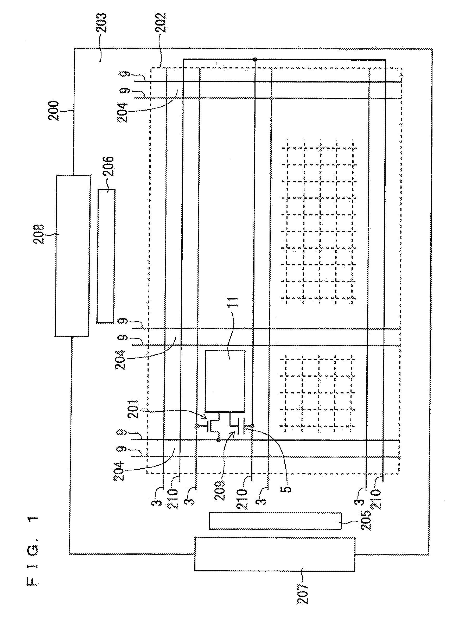
[0034]FIG. 1 is a plan view illustrating a configuration of a TFT substrate according to a first preferred embodiment. The TFT substrate according to the first preferred embodiment is an active matrix substrate including a plurality of thin film transistors (TFTs), which serve as a switching element and are arranged in a matrix. In the present preferred embodiment, the TFT substrate for a liquid crystal display (LCD) that is a planar display device (flat panel display) will be described as one example.

[0035]A TFT substrate 200 is divided into a display region 202 in which pixels 204, each having a TFT 201, are arranged in a matrix and a frame region 203 externally enclosing the display region 202.

[0036]A plurality of gate lines (scanning signal lines) 3 and a plurality of source lines (display signal lines) 9 are arranged on the display region 202. The plurality of gate lines 3 are arranged parallel to one another, and the plurality of source lines 9 are also arranged parallel to on...

second preferred embodiment

[0096]FIGS. 8 and 9 are views illustrating a configuration of a TFT substrate 200 according to a second preferred embodiment. In these drawings, the components same as those in FIGS. 2 and 3 are identified by the same numerals.

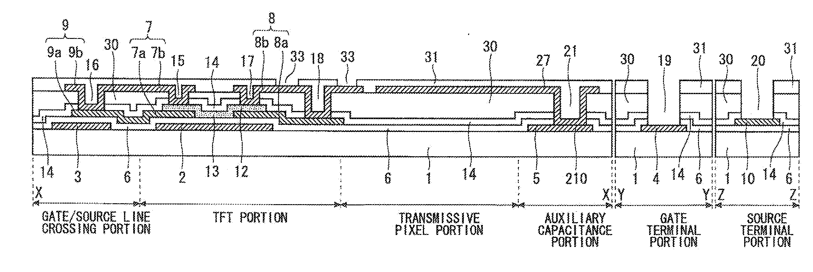
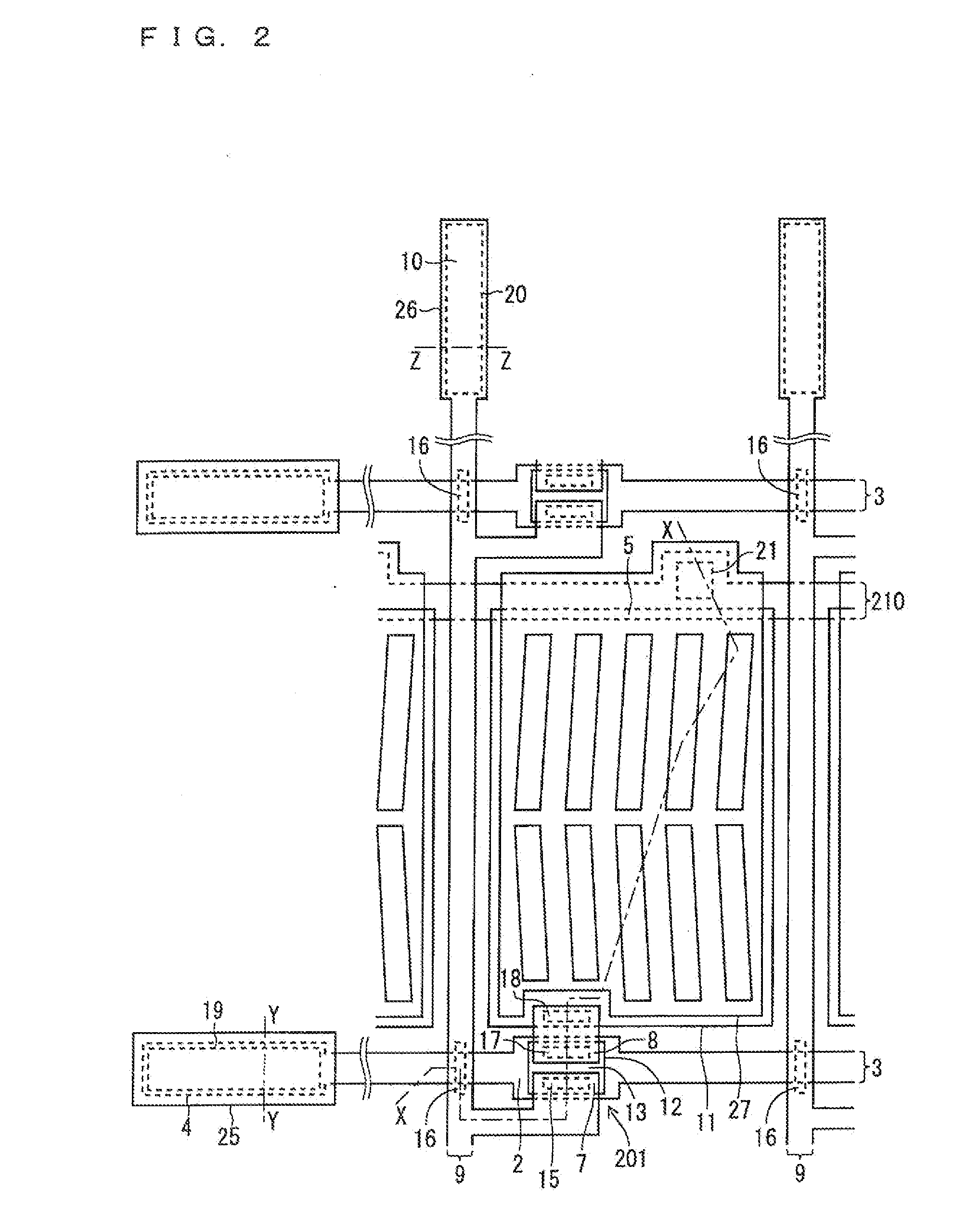
[0097]FIG. 8 is a view illustrating a planar configuration of an essential part including a pixel 204 on the TFT substrate 200 using the FFS system, and FIG. 9 is a view illustrating its sectional configuration. FIG. 9 illustrates the sections corresponding to X-X line, Y-Y line, and Z-Z line in FIG. 8.

[0098]The section along X-X line corresponds to a formation region of the pixel 204 (pixel portion). The section along Y-Y line corresponds to a formation region of a gate terminal 4 and a gate terminal pad 25 (gate terminal portion), and the section along Z-Z line corresponds to a formation region of a source terminal 10 and a source terminal pad 26 (source terminal portion). In addition, the section of the pixel portion along X-X line includes a “gate / source l...

third preferred embodiment

[0154]The second preferred embodiment describes the configuration in which the interdigital common electrode having a slit is arranged above the plate-like pixel electrode. However, a configuration in which an interdigital pixel electrode is arranged above a plate-like common electrode may be employed. In a third preferred embodiment, the case where the present invention is applied to a TFT substrate having the latter configuration will be described.

[0155]FIGS. 16 and 17 are views illustrating a configuration of a TFT substrate 200 according to the third preferred embodiment. In these drawings, the components same as those in FIGS. 2 and 3 are identified by the same numerals.

[0156]FIG. 16 is a view illustrating a planar configuration of an essential part including a pixel 204 on the TFT substrate 200 using the FFS system, and FIG. 17 is a view illustrating its sectional configuration. FIG. 17 illustrates the sections corresponding to X-X line, Y-Y line, and Z-Z line in FIG. 16.

[0157...


PUM


Abstract

A TFT substrate includes a TFT including a source electrode having a lower source electrode and an upper source electrode, which are electrically connected to each other, and a drain electrode having a lower drain electrode and an upper drain electrode, which are electrically connected to each other. The lower source electrode and the lower drain electrode are in contact with a lower surface of the semiconductor film, and the upper source electrode and the upper drain electrode are in contact with an upper surface of the semiconductor film.

Description

BACKGROUND OF THE INVENTION[0001]1. Field of the Invention[0002]The present invention relates to a thin film transistor substrate used in a display device or the like.[0003]2. Description of the Background Art[0004]A TFT active matrix substrate (thin film transistor substrate; hereinafter referred to as a “TFT substrate”) using a thin film transistor (hereinafter referred to as a “TFT”) as a switching element is used in an electrooptical device such as a display device (liquid crystal display) using liquid crystal. A semiconductor device such as a TFT has features of reduced power consumption and thin size, and it has actively been applied to a flat panel display that replaces a CRT (Cathode Ray Tube) by utilizing these features.[0005]An electrooptical element for a liquid crystal display (LCD) includes a simple matrix LCD and a TFT-LCD using a TFT as a switching element. The TFT-LCD is particularly more excellent than the CRT or the simple matrix LCD in portability and display qual...

Claims


Application Information

Patent Timeline
Patent Type & Authority Applications(United States)
IPC IPC(8): H01L29/786H01L29/66
CPCH01L29/66969H01L29/7869H01L27/1225H01L27/124H01L27/1248H01L27/1255H01L29/41733H01L27/1259H01L29/42384
Inventor NAGAYAMA, KENSUKEINOUE, KAZUNORIITO, YASUYOSHIISHIGA, NOBUAKITSUMURA, NAOKIYANO, SHINICHI
Owner TRIVALE TECH
Learn More