Polishing method and polishing apparatus

a technology of polishing apparatus and polishing method, which is applied in the direction of lapping machines, grinding machine components, manufacturing tools, etc., can solve the problems of inability to measure the thickness at the same position under the same conditions, and the film thickness measuring device incorporated in the cmp apparatus may fail to measure the thickness, so as to prevent the failure of detection of the polishing end point

US20140323016A1Active Publication Date: 2014-10-30EBARA CORP
24 Cites 3 Cited by

Patent Information

Authority / Receiving Office
US · United States
Patent Type
Applications(United States)
Current Assignee / Owner
Publication Date
2014-10-30

Smart Images

  • Figure 1
    Figure 1
  • Figure 2
    Figure 2
  • Figure 3
    Figure 3
Patent Text Reader

Abstract

A method of polishing a substrate is disclosed. The method includes irradiating the substrate with light; measuring intensity of the reflected light; producing spectral waveform representing relationship between relative reflectance and wavelength of the light; performing a Fourier transform process on the spectral waveform to determine a thickness of the film and a corresponding strength of frequency component; determining whether the determined thickness of the film is reliable or not by comparing the strength of frequency component with a threshold value; calculating a defective data rate representing a proportion of the number of unreliable measured values to the total number of measured values; and changing the threshold value based on the defective data rate.
Need to check novelty before this filing date? Find Prior Art

Description

CROSS REFERENCE TO RELATED APPLICATION

[0001] This application claims priority to Japanese Patent Application No, 2013-092183 filed Apr. 25, 2013, the entire contents of which are hereby incorporated by reference.BACKGROUND

[0002] Semiconductor devices are fabricated through several processes including a process of polishing a dielectric film, e.g., SiO2, and a process of polishing a meta film, e.g., copper or tungsten. Fabrication processes of backside illumination CMOS sensor and through-silicon via (TSV) include a process of polishing a silicon layer (silicon wafer), in addition to the polishing processes of the dielectric film and the metal film.

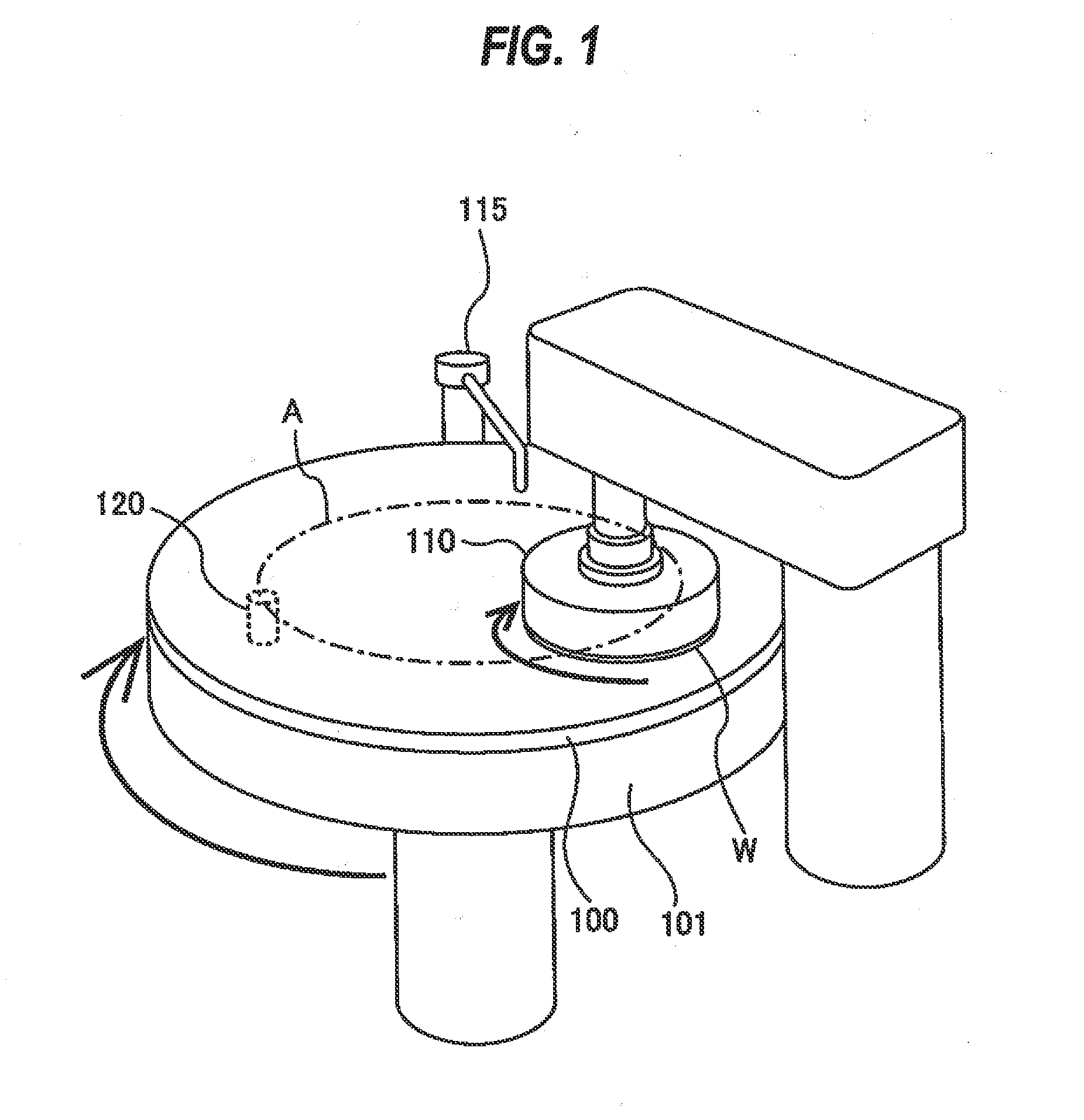
[0003] Polishing of the wafer is terminated when a thickness of a film (e.g., the dielectric film, the metal film, or the silicon layer), constituting a wafer surface, has reached a predetermined target value. CMP (Chemical Mechanical Polishing) apparatus is used for polishing the wafer. FIG. 1 is a schematic view of the CMP apparatus. The CM...

Examples

Embodiment Construction

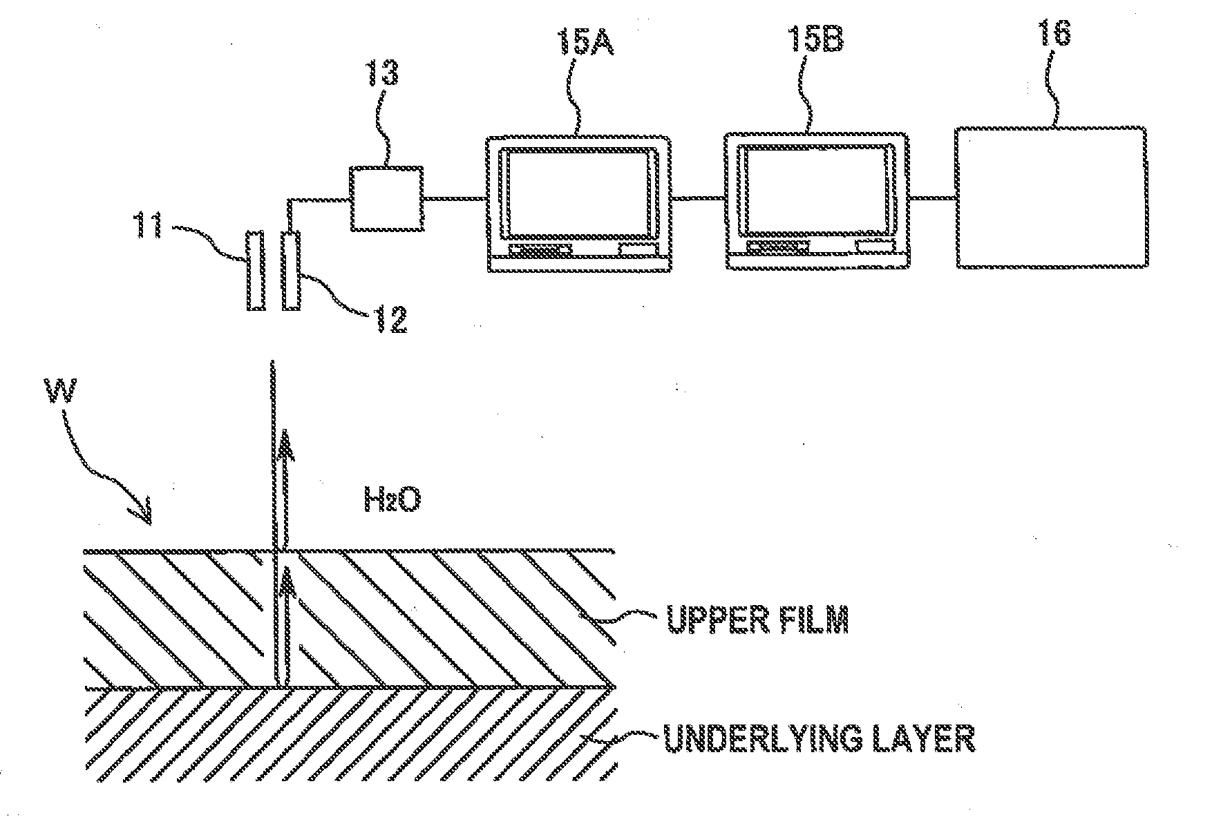
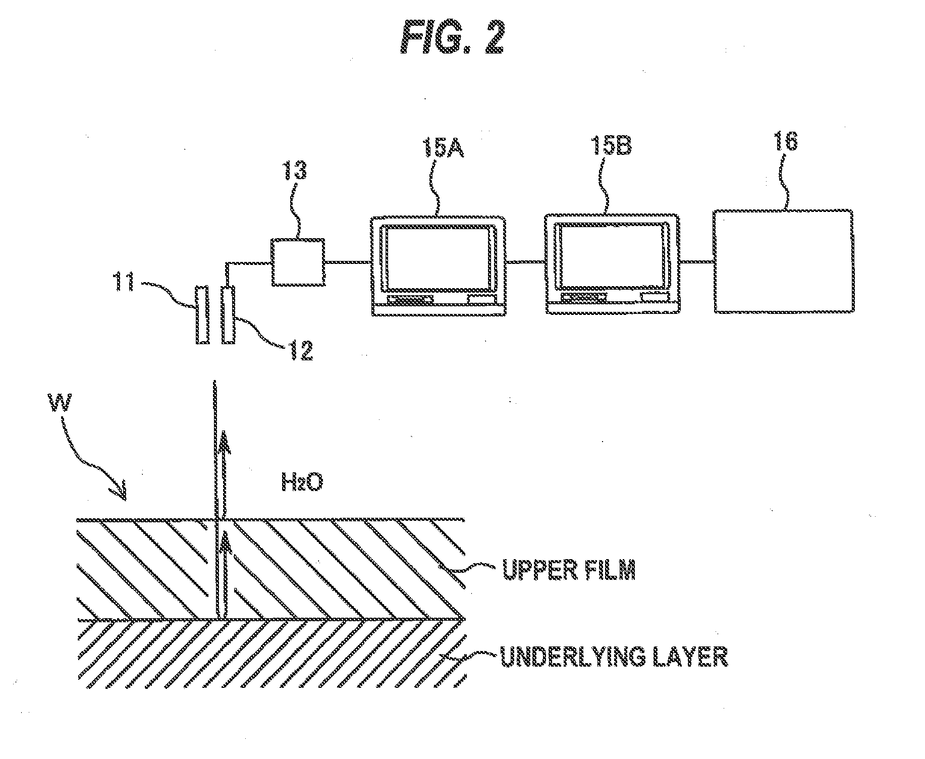
[0046]Embodiments of the present invention will be described below with reference to the drawings. FIG. 2 is a schematic view for illustrating the principle of an optical polishing end point detection method, and FIG. 3 is a plan view showing positional relationship between wafer and polishing table. As shown in FIG. 2, a wafer W has an underlying layer and a film formed on the underlying layer. The wafer W is held by a top ring (not shown in FIGS. 2 and 3) and rotated about its central axis as shown in FIG. 3. A surface of the wafer W is pressed by the top ring against a polishing pad 22 on a rotating polishing table 20, so that the film of the wafer W is polished by sliding contact with the polishing pad 22, which is a polishing tool having a polishing surface for polishing the wafer W. A grindstone (or fixed abrasive) may be used as the polishing tool, instead of the polishing pad 22.

[0047]An irradiator 11 and an optical receiver 12 are disposed in the polishing table 20 and are ...