Trench type power transistor device

a power transistor and clamping technology, applied in the direction of semiconductor devices, basic electric elements, electrical equipment, etc., can solve the problems of lowering device performance, high miller capacitance, inevitable switching losses, etc., and achieve the effect of reducing the capacitance and switching losses of the device and improving the performance of the devi

Inactive Publication Date: 2014-11-06
ANPEC ELECTRONICS CORPORATION
View PDF1 Cites 10 Cited by
  • Summary
  • Abstract
  • Description
  • Claims
  • Application Information

AI Technical Summary

Benefits of technology

[0009]It is therefore one objective of the invention to provide a trench type power transistor device and a method thereof so that a power transistor device with low Miller capacitance and high voltage sustaining ability can be obtained.
[0012]The present invention provides a method for fabricating a trench type power transistor device, which has first doped diffusion layers partially overlapped by the gate conductive layer along a vertical direction. The first doped diffusion layers can be fabricated by first filling a first through hole with electrically insulating dopant source layer and then performing a thermal drive-in process so that conductive dopants inside the dopant source layer can diffuse into an epitaxial layer. As a result, the first doped diffusion layers with the first conductivity type and the epitaxial layer with the second conductivity type are alternately arranged and can construct a super junction structure. In addition, since the dopant source layer having insulating properties is located under the gate conductive layer, a parasitical capacitor between the gate and the drain of the trench type power transistor device can be reduced, and the Miller capacitance and switching losses in the device can be reduced effectively. As a result, the performance of the device is improved.

Problems solved by technology

However, since an overlapped area between a gate structure and an N-type epitaxial layer (also called drain region) in this power transistor device is relatively high, and the thickness of a gate dielectric layer between the gate structure and the N-type epitaxial layer is relatively thin, these will cause relatively high Miller capacitance and produce inevitable switching losses.
As a result, the performance of the devices is lowered.

Method used


Image

  • Trench type power transistor device
  • Trench type power transistor device
  • Trench type power transistor device

Examples


Embodiment Construction

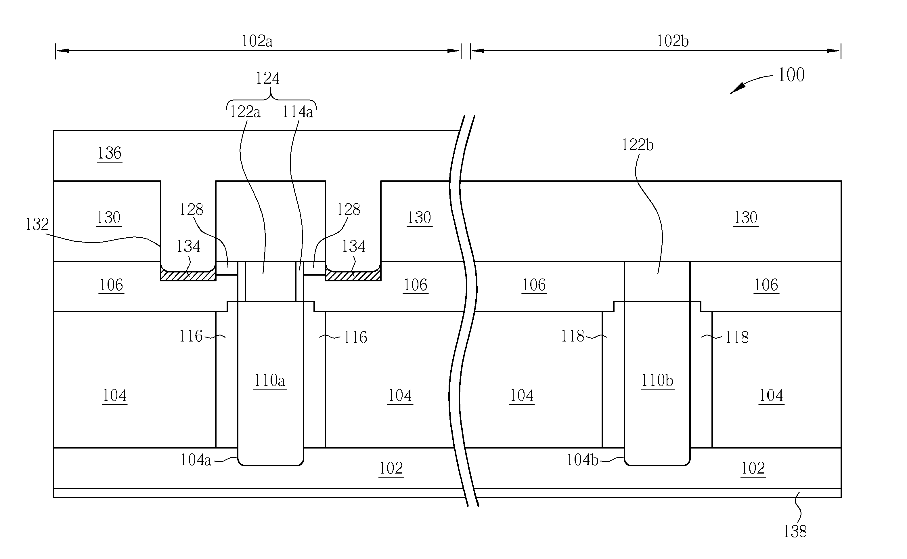
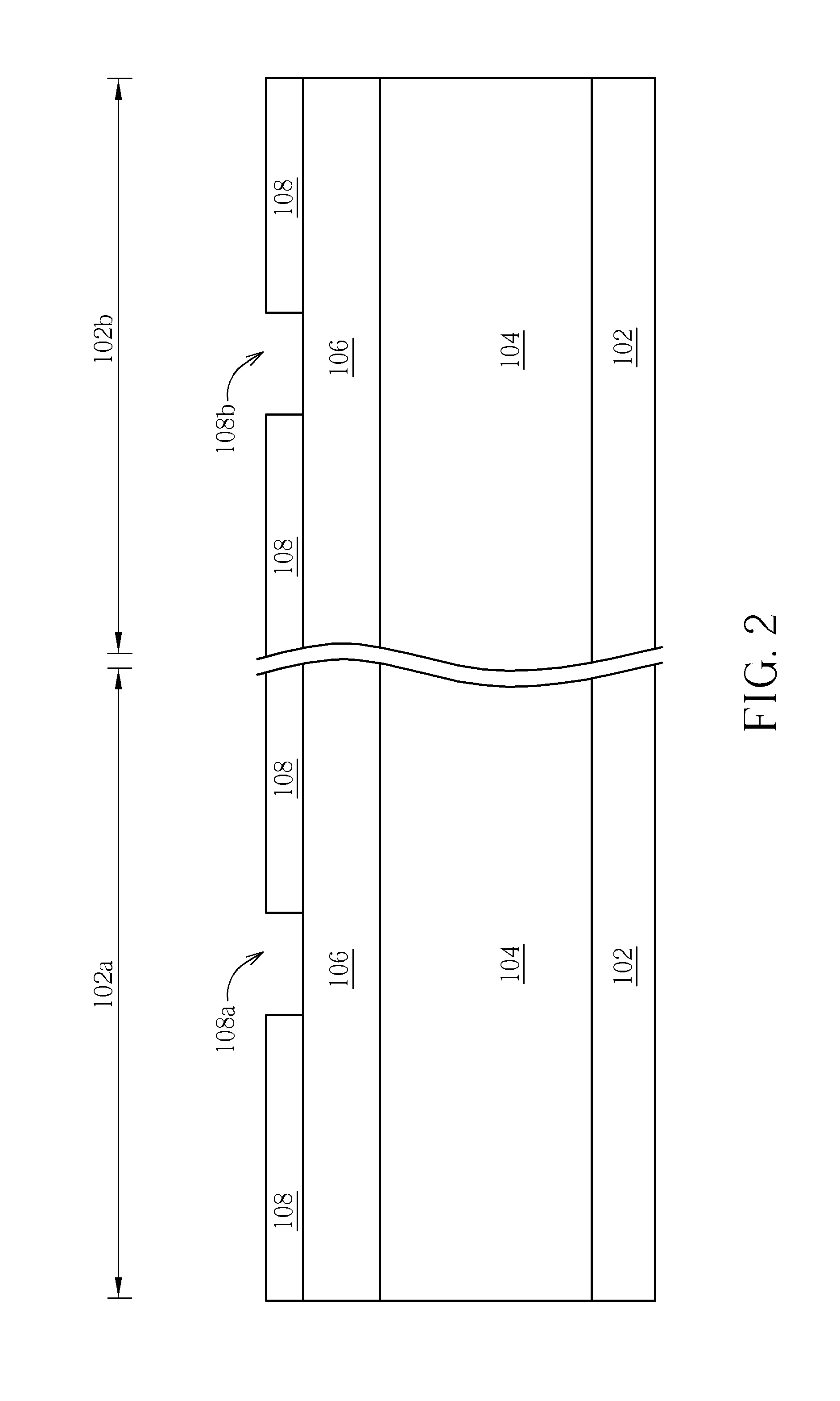
[0017]Please refer to FIG. 2 to FIG. 9. FIGS. 2-9 are schematic, cross-sectional diagrams showing a method for fabricating a trench type power transistor device according to one embodiment of the invention, wherein FIG. 9 is a schematic, cross-sectional diagram showing a structure of the trench type power transistor device. As shown in FIG. 2, a substrate 102 having a first conductivity type and having an active region 102a and a termination region 102b is provided, wherein the active region 102a is used to accommodate active devices and the termination region 102b is used to accommodate a termination structure. Then, an epitaxial layer 104 having a second conductivity type is formed on the substrate 104 through performing an epitaxial growth process, wherein the second conductivity type is different from the first conductivity type. After the formation of the epitaxial layer 104, an oxide layer (not shown) is then formed on the epitaxial layer 104 through a deposition process. With...


PUM


Abstract

The present invention provides a trench type power transistor device including a substrate, an epitaxial layer, a doped diffusion region, a doped source region, and a gate structure. The substrate, the doped diffusion region, and the doped source region have a first conductivity type, and the substrate has an active region and a termination region. The epitaxial layer is disposed on the substrate, and has a second conductivity type. The epitaxial layer has a through hole disposed in the active region. The doped diffusion region is disposed in the epitaxial layer at a side of the through hole, and is in contact with the substrate. The doped source region is disposed in the epitaxial layer disposed right on the doped diffusion region, and the gate structure is disposed in the through hole between the doped diffusion region and the doped source region.

Description

CROSS REFERENCE TO RELATED APPLICATIONS[0001]This application is a divisional application of and claims the benefit of U.S. patent application Ser. No. 13 / 543,877, filed Jul. 8, 2012.BACKGROUND OF THE INVENTION[0002]1. Field of the Invention[0003]The present invention generally relates to the field of semiconductor power devices. More particularly, the present invention relates to a trench type power transistor device having super-junction structures and a method thereof.[0004]2. Description of the Prior Art[0005]Power devices are used in power management; for example, in switchable power supplies, management integrated circuits in the core or in the peripheral region of computers, backlight power supplies, and in electric motor controls. The type of power devices described above include an insulated gate bipolar transistor (IGBT), a metal-oxide-semiconductor field effect transistor (MOSFET), a bipolar junction transistor (BJT) and so forth.[0006]Please refer to FIG. 1, which is a s...

Claims


Application Information

Patent Timeline
Patent Type & Authority Applications(United States)
IPC IPC(8): H01L29/06H01L29/739
CPCH01L29/0634H01L29/7395H01L21/2255H01L29/0886H01L29/1095H01L29/41766H01L29/423H01L29/66348H01L29/66727H01L29/66734H01L29/7397H01L29/7811H01L29/7813
Inventor LIN, YUNG-FAHSU, SHOU-YIWU, MENG-WEICHANG, CHIA-HAO
Owner ANPEC ELECTRONICS CORPORATION
Why Eureka
Try Eureka