Magnetic memory devices

a magnetic memory and memory cell technology, applied in the field of spin transferorque magneticrandomaccess memory (mram) cells, can solve the problems of uncontrollable re-crystallization, uniformity, and typical mtj damage or partial damage, and achieve the effect of reducing undesirable heating

Active Publication Date: 2014-11-06
GUO YIMIN
View PDF3 Cites 28 Cited by
  • Summary
  • Abstract
  • Description
  • Claims
  • Application Information

AI Technical Summary

Benefits of technology

[0013]The present invention comprises a magnetoresistive memory cell having a heat barrier for reducing undesirable heating of the magnetic tunneling junction during pulsed laser heating annealing of upper copper bit lines.
[0016]In a laser thermal annealing, a short wavelength of a laser has a shallow thermal penetration depth which reduces direct heating to the lower magnetic materials. In this invention, a dielectric thermal buffer or barrier layer having a low thermal conductivity is deposited between a thin top electrode of the MTJ element and a bit line, while the VIA electrically connecting the top electrode and the bit line has a vertical distance away from the location of the MTJ element. Thus, a high thermal resistance from the bit line to the MTJ element is achieved, and the temperature rise of the MTJ element is much smaller than that of the bit line during a pulsed laser thermal annealing. As the temperature of the MTJ element during the laser thermal annealing of bit line copper layer is controlled under 300-degree C., there is no damage on MTJ and magnetic property.

Problems solved by technology

However re-crystallization is not under control and not uniform in this case and depends also on the width of the Cu lines.
Microstructural, mechanical and contamination results show that rapid thermal anneals at 400° C. offer performances that are similar to longer furnace anneals at the same temperature, whereas 250° C. anneals are insufficient and 300° C. anneals are marginal.
A typical MTJ would be damaged or partially damaged by a conventional uniform high temperature annealing of copper lines by long batch furnace thermal treatments.

Method used


Image

  • Magnetic memory devices
  • Magnetic memory devices
  • Magnetic memory devices

Examples


Embodiment Construction

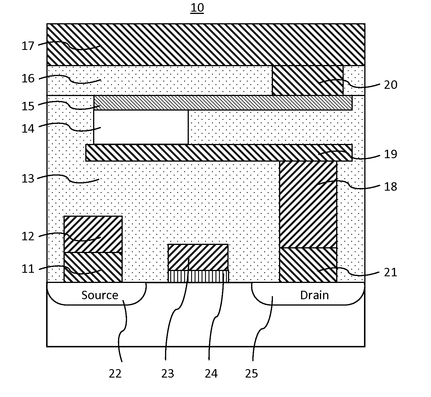
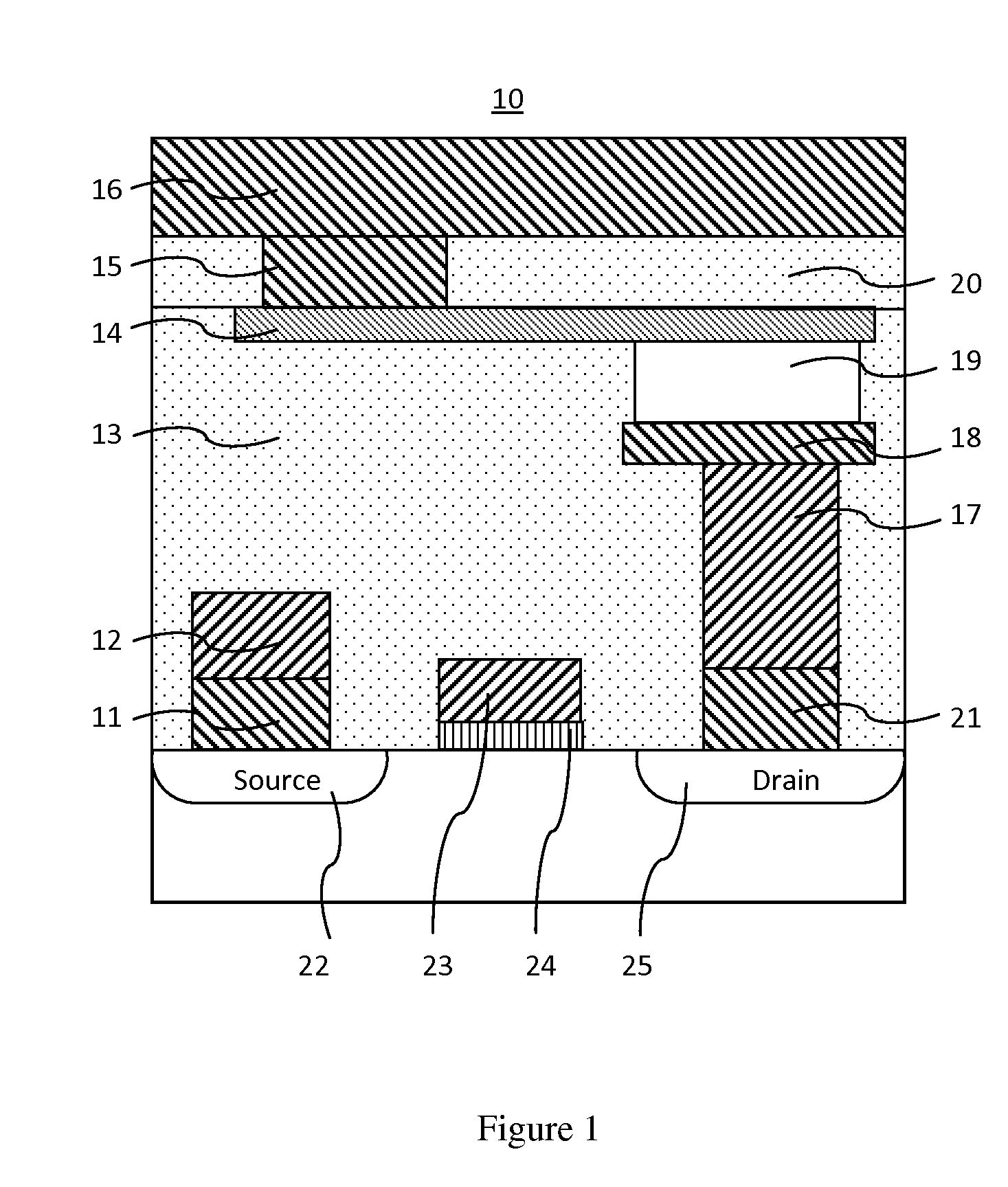
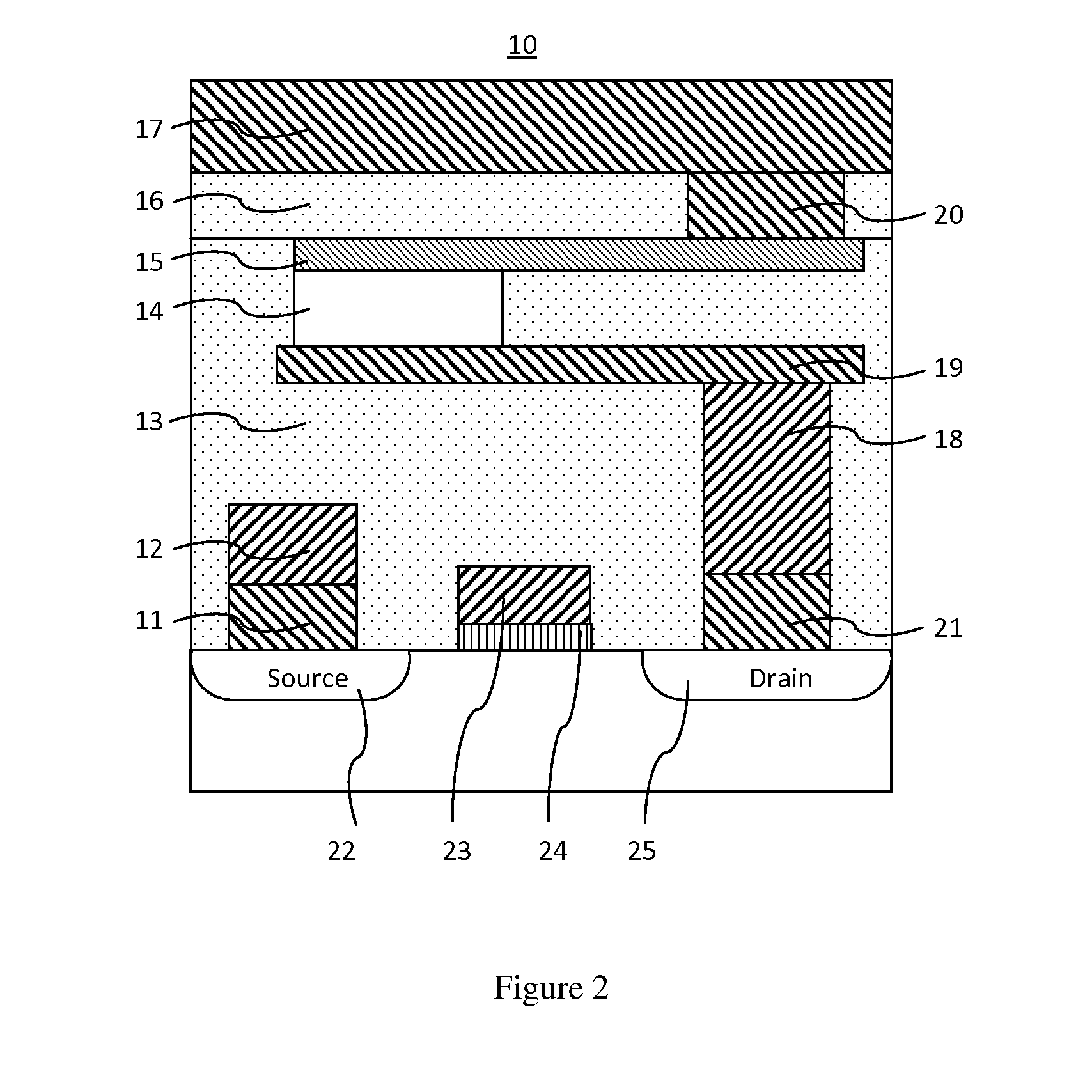
[0020]In general, according to each embodiment, there is provided a magnetoresistive memory cell comprising:

[0021]a bottom electrode provided on a surface of a substrate connecting to a VIA of a select transistor;

[0022]a patterned MTJ stack consisting of a seed layer provided on the top surface of the bottom electrode, an MTJ multilayer provided on the top surface of the seed layer and a cap layer provided on the top surface of the MTJ multilayer;

[0023]a top electrode provided on the surface of the MTJ stack;

[0024]a dielectric thermal barrier layer provided on the top surface of the top electrode;

[0025]a bit-line VIA provided on the surface of the top electrode and surrounded by the dielectric thermal barrier layer and having a vertical distance away from the MTJ stack;

[0026]a bit line provided on the top surface of the dielectric thermal barrier layer and electrically connecting to the bit-line VIA.

[0027]An exemplary embodiment includes a spin-transfer-torque magnetoresistive memor...


PUM


Abstract

A STT-MRAM comprises apparatus and a method of manufacturing a plurality of magnetoresistive memory element having a dielectric thermal buffer layer between a thin top electrode of the MTJ element and a bit line, and a bit-line VIA electrically connecting the top electrode and the bit line having a vertical distance away from the location of the MTJ stack. In a laser thermal annealing, a short wavelength of a laser has a shallow thermal penetration depth and a high thermal resistance from the bit line to the MTJ stack only causes a temperature rise of the MTJ stack being much smaller than that of the bit line. As the temperature of the MTJ element during the laser thermal annealing of bit line copper layer is controlled under 300-degree C., possible damages on MTJ and magnetic property can be avoided.

Description

RELATED APPLICATIONS[0001]This application claims the priority benefit of U.S. Provisional Application No. 61,820,101 filed on May 6, 2013, which is incorporated herein by reference.BACKGROUND OF THE INVENTION[0002]1. Field of the Invention[0003]This invention relates generally to a spin-transfer-torque magnetic-random-access memory (MRAM) cell having a heat buffer (barrier) layer for reducing undesirable heating of the magnetic tunneling junction during pulsed laser heating annealing of upper copper bit lines.[0004]2. Description of the Related Art[0005]In recent years, magnetic random access memories (hereinafter referred to as MRAMs) using the magnetoresistive effect of ferromagnetic tunnel junctions (also called MTJs) have been drawing increasing attention as the next-generation solid-state nonvolatile memories that can also cope with high-speed reading and writing. A ferromagnetic tunnel junction has a three-layer stack structure formed by stacking a recording layer having a ch...

Claims


Application Information

Patent Timeline
Patent Type & Authority Applications(United States)
IPC IPC(8): G11C11/16H01L43/12
CPCH01L43/12G11C11/161H10B61/22H10N50/01H10N50/10H10B61/00H10N50/80H10N50/85
Inventor GUO, YIMIN
Owner GUO YIMIN
Why Eureka
Try Eureka