Mask blank substrate, substrate with multilayer reflection film, transmissive mask blank, reflective mask blank, transmissive mask, reflective mask, and semiconductor device fabrication method

a semiconductor device and substrate technology, applied in the field of mask blank substrates, can solve the problems of defect information on the mask blank substrate, the inspection cannot be completed to the end, and the lithography process is becoming prominent, etc., to achieve suppress false defects, facilitate the detection of critical defects, and high reflectance

Active Publication Date: 2014-11-06
HOYA CORP
View PDF1 Cites 27 Cited by
  • Summary
  • Abstract
  • Description
  • Claims
  • Application Information

AI Technical Summary

Benefits of technology

[0071]The mask blank substrate, a substrate with a multilayer reflective film, the transmissive mask blank, the reflective mask blank, the transmissive mask and the reflective mask according to the invention permit detection of false defects originating from the surface roughness of a substrate and a film to be suppressed in defect inspection using a high-sensitivity defect inspection apparatus, and facilitate the detection of critical defects such as foreign matters and scratches. In the mask blank substrate, the substrate with a multilayer reflective film, the reflective mask blank and the reflective mask for use in EUV lithography, in particular, the multilayer reflective film formed on the main surface of the substrate provides high reflectance while suppressing false defects.
[0072]According to the above-described method of manufacturing a semiconductor device, a reflective mask or a transmissive mask from which critical defects such as a foreign matter or scratches is removed can be used in defect inspection using a high-sensitivity defect inspection apparatus, so that a transfer pattern such as a circuit pattern to be transferred on a resist film formed on a transferred substrate such as a semiconductor substrate is free of defects. This makes it possible to manufacture a semiconductor device having a fine and high-precision circuit pattern.
[0073]A mask blank substrate according to the present invention is described as follows.
[0074]FIG

Problems solved by technology

As described above, as a demand for miniaturization in the lithography process increases, problems in the lithography process are becoming prominent.
One of the problems concerns defect information on a mask blank substrate or the like, which are used in the lithography process.
Because the detection sensitivity of the high-sensitivity defect inspection apparatus described above is high, however, many false defects are detected in defect inspection of the main surface of the substrate even when the smoothness in compliance with Rms and Rmax becomes higher from the viewpoint of the improvement on the defect quality, raising a problem such that the defect inspection cannot be performed to the end.
The false defect mentioned herein refers to a tolerable irregularity (unevenness) on the substrat

Method used


Image

  • Mask blank substrate, substrate with multilayer reflection film, transmissive mask blank, reflective mask blank, transmissive mask, reflective mask, and semiconductor device fabrication method
  • Mask blank substrate, substrate with multilayer reflection film, transmissive mask blank, reflective mask blank, transmissive mask, reflective mask, and semiconductor device fabrication method
  • Mask blank substrate, substrate with multilayer reflection film, transmissive mask blank, reflective mask blank, transmissive mask, reflective mask, and semiconductor device fabrication method

Examples


example 1

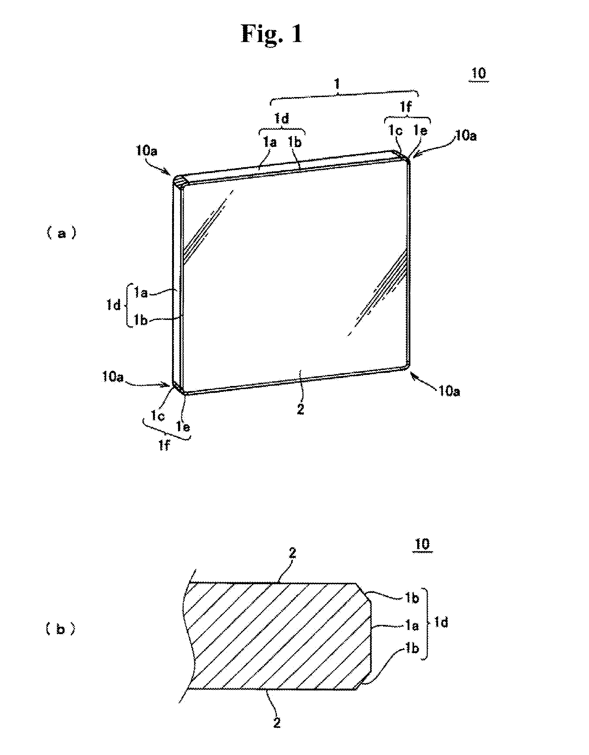
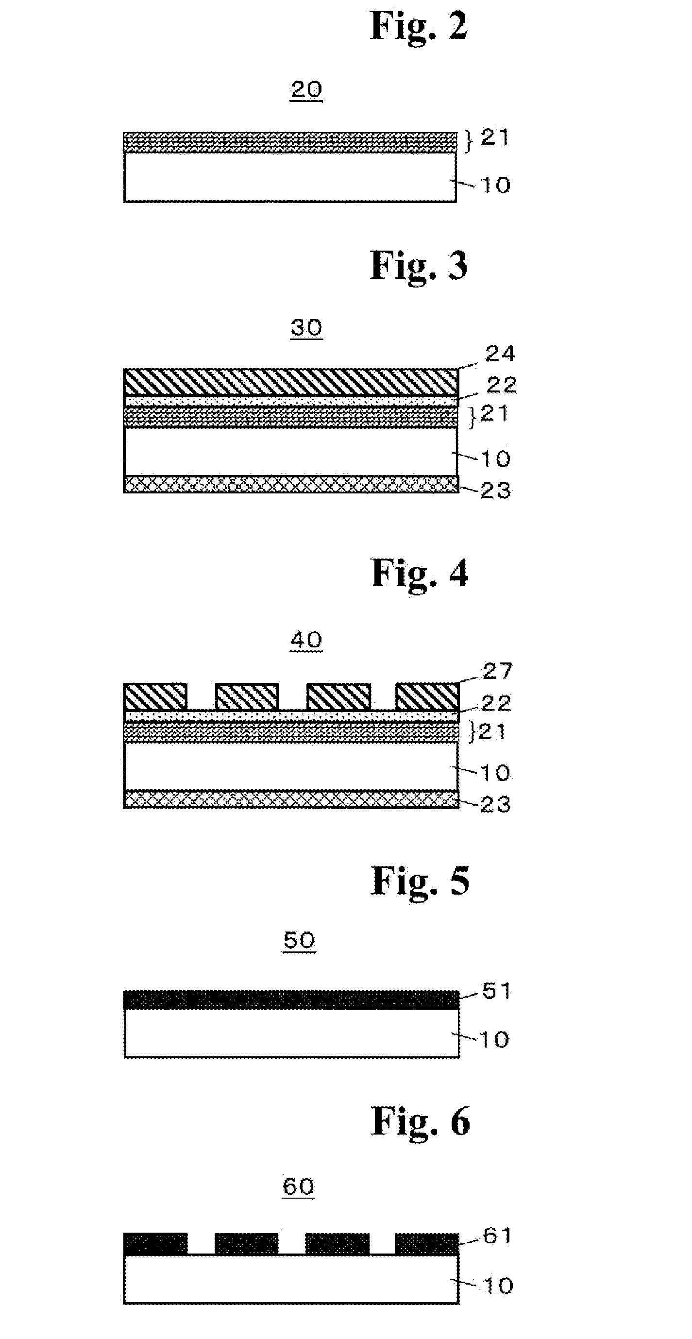
[0143]First, Example 1 for the mask blank substrate and the substrate with a multilayer reflective film for EUV exposure according to the invention, and the reflective mask blank and the reflective mask for EUV exposure is described.

[0144]For a mask blank substrate 10, a SiO2—TiO2 glass substrate with a size of 152.4 mm×152.4 mm and a thickness of 6.35 mm was prepared, and the top and bottom sides of the glass substrate were polished step by step with cerium oxide abrasive particles or colloidal silica abrasive grains using a double-side polishing apparatus. Then, the glass substrate was subjected to a surface treatment with hydrosilicofluoric acid of a low concentration. The surface roughness of the surface of the glass substrate provided through the treatment was measured with an atomic force microscope, and the root mean square roughness (Rms) was 0.15 nm.

[0145]The surface shapes (surface state, flatness) of areas of 148 mm×148 mm at the top and bottom sides of the glass substrat...

example 2

Fabrication of Mask Blank Substrate

[0180]An SiO2—TiO2 glass substrate with a size of 152.4 mm×152.4 mm and a thickness of 6.35 mm was prepared as the mask blank substrate 10 for EUV exposure, and the top and bottom sides of the glass substrate were subjected to processes from polishing with the double-side polishing apparatus to the local surface treatment by magnetic viscoelastic fluid polishing, with the same manner as in Example 1.

[0181]Thereafter, noncontact polishing of the top and bottom sides of the glass substrate was performed as finish polishing in the local surface treatment. In Example 2, EEM (Elastic Emission Machining) was performed as the non-contact polishing. The EEM was performed under the following processing conditions.

[0182]working fluid (first stage): aqueous alkaline solution (NaOH)+fine particles (concentration: 5 wt %)

[0183]working fluid (second stage): pure water

[0184]fine powder particles: colloidal silica, average particle size: about 100 nm

[0185]rotation...

example 3

Fabrication of Mask Blank Substrate

[0200]In this Example 3, a SiO2—TiO2 glass substrate with a size of 152.4 mm×152.4 mm and a thickness of 6.35 mm was prepared as the mask blank substrate 10 for EUV exposure, with the same manner as in Examples 1 and 2, and the mask blank substrate 10 for EUV exposure was fabricated through substantially the same processes as taken in Example 2. It is noted that in Example 3, EEM processing at the second stage using pure water as the working fluid was omitted in finish polishing in the local surface treatment in Example 2. The mask blank substrate 10 was fabricated in the same manner as Example 2 except for this process.

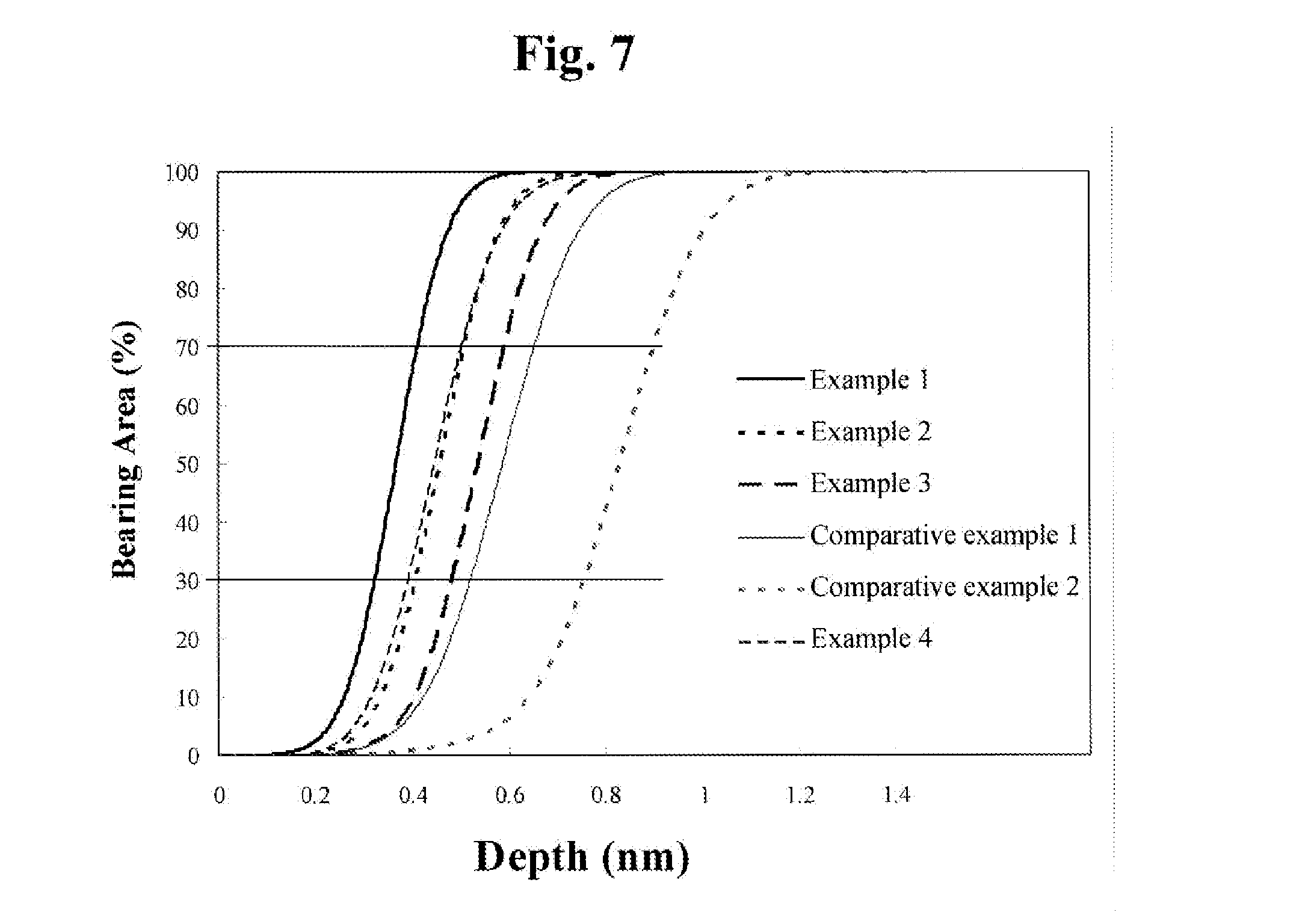
[0201]An area of 1 μm×1 μm at an arbitrary location in the transfer-pattern forming area (132 mm×132 mm) on the main surface of the mask blank substrate 10 for EUV exposure provided by Example 3 was measured with an atomic force microscope; the root mean square roughness (Rms) was 0.11 nm, and the maximum height (Rmax) was 0.98 nm. ...


PUM


Abstract

Disclosed is a mask blank substrate for use in lithography, wherein a main surface of the substrate satisfies a relational equation of (BA70−BA30)/(BD70−BD30)≧350 (%/nm), and has a maximum height (Rmax)≦1.2 nm in a relation between a bearing area (%) and a bearing depth (nm) obtained by measuring, with an atomic force microscope, an area of 1 μm×1 μm in the main surface on the side of the substrate where a transfer pattern is formed, wherein BA30 is defined as a bearing area of 30%, BA70 is defined as a bearing area of 70%, and BD70 and BD30 are defined to respectively represent bearing depths for the bearing area of 30% and the bearing area of 70%.

Description

TECHNICAL FIELD[0001]The present invention relates to a mask blank substrate, a substrate with a multilayer reflective film, a transmissive mask blank, a reflective mask blank, a transmissive mask, a reflective mask, and a method of manufacturing a semiconductor device, which ensure suppression of false defects (pseudo defects, nuisance defects) originating from the surface roughness of a substrate and a film in defect inspection using a high-sensitivity defect inspection apparatus, and facilitate the detection of critical defects such as foreign matters and scratches.BACKGROUND ART[0002]Generally, in the process of manufacturing a semiconductor device, fine patterns are formed using photolithography. A number of transfer masks called photomasks are normally used in forming the fine patterns. This transfer mask is generally a fine pattern formed by a metal thin film or the like and provided on a transparent glass substrate, and photolithography is also used in the fabrication of the...

Claims


Application Information

Patent Timeline
IPC IPC(8): G03F1/50
CPCG03F1/50G03F1/22G03F1/60H01L21/0274G03F7/2004H01L21/0332H01L21/0334
Inventor HAMAMOTO, KAZUHIROORIHARA, TOSHIHIKOKOZAKAI, HIROFUMIUSUI, YOUICHISHOKI, TSUTOMUHORIKAWA, JUNICHI
Owner HOYA CORP
Why Eureka
Try Eureka