

Packaged overvoltage protection circuit for triggering thyristors
a protection circuit and thyristor technology, applied in the field of breakover diodes, can solve the problems of thyristor being negatively biased, thyristor being able to be switched off, and the current is not sufficient to turn on transistors, so as to reduce the ill effects of switching voltage spikes and limit the magnitude of triggering curren
- Summary
- Abstract
- Description
- Claims
- Application Information
AI Technical Summary
Benefits of technology
Problems solved by technology
Method used
Image

Examples
Embodiment Construction
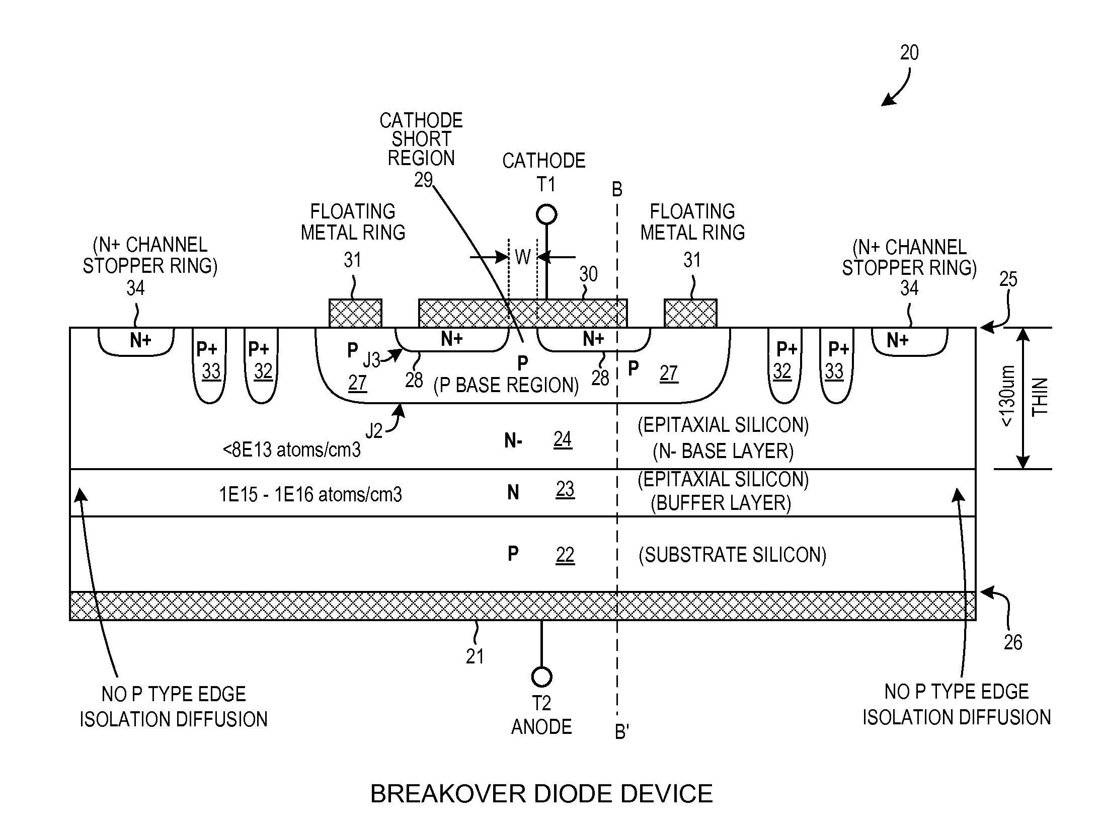
[0054]Reference will now be made in detail to background examples and some embodiments of the invention, examples of which are illustrated in the accompanying drawings. In the description and claims below, when a first object is referred to as being disposed “over” or “on” a second object, it is to be understood that the first object can be directly on the second object, or an intervening object may be present between the first and second objects. Similarly, terms such as “upper”, “top”, “up”, “down”, and “bottom” are used herein to describe relative orientations between different parts of the structure being described, and it is to be understood that the overall structure being described can actually be oriented in any way in three-dimensional space. The notations N+, N−, N, P+, and P are only relative, and are to be considered in context, and do not denote any particular dopant concentration range.
[0055]FIG. 7 is a cross-sectional diagram of a breakover diode (BOD) device 20 in ac...
PUM
 Abstract
Description
Claims
Application Information