
Contact-free photomixing probe for device and integrated circuit measurement or characterization

a photomixing probe and integrated circuit technology, applied in the direction of resistance/reactance/impedence, instruments, material analysis, etc., can solve the problems of inacceptable device characterization, and large deformation of the instantaneous signal-to-noise ratio compared to a coherent transceiver, etc., to achieve low thz dielectric loss, reduce the effect of thz dielectri

Active Publication Date: 2014-11-27
WRIGHT STATE UNIVERSITY
View PDF2 Cites 11 Cited by
  • Summary
  • Abstract
  • Description
  • Claims
  • Application Information

AI Technical Summary

Benefits of technology

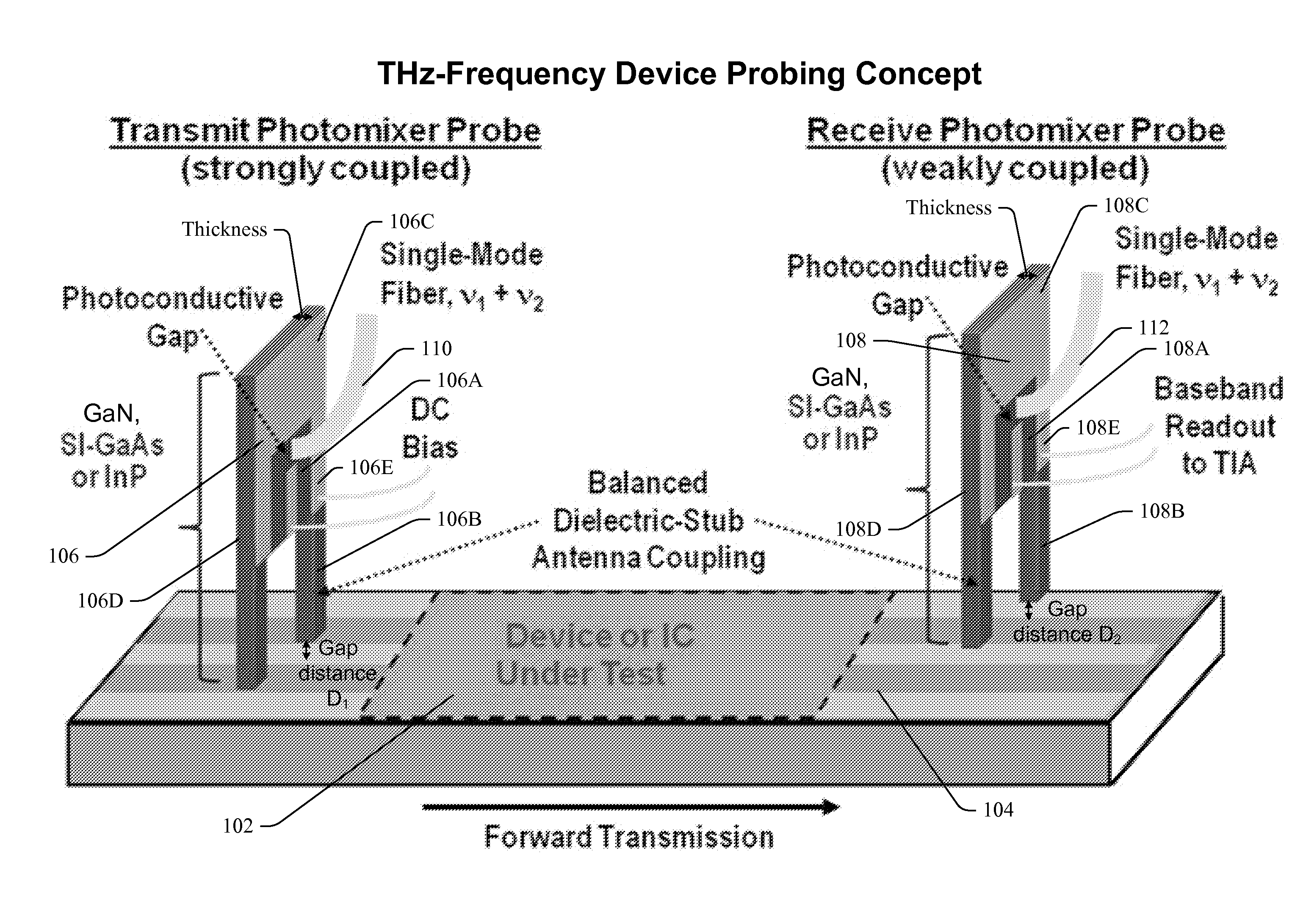
This patent describes a method of measuring balanced THz transmission lines using contact-free, ac-coupled probes that are made from high-resistivity substrates such as silicon or gallium arsenide. The probes have a fork-like or orthorhombic shape and are designed to minimize loss. The ac coupling is achieved through polarization current, which naturally occurs in these materials due to their high dielectric constant and low THz dielectric loss. Unlike metal-to-metal coupling, which becomes increasingly lossy with frequency, dielectric coupling improves approximately linearly with frequency. Overall, this method provides a more efficient and accurate way to measure balanced THz transmission lines.

Problems solved by technology

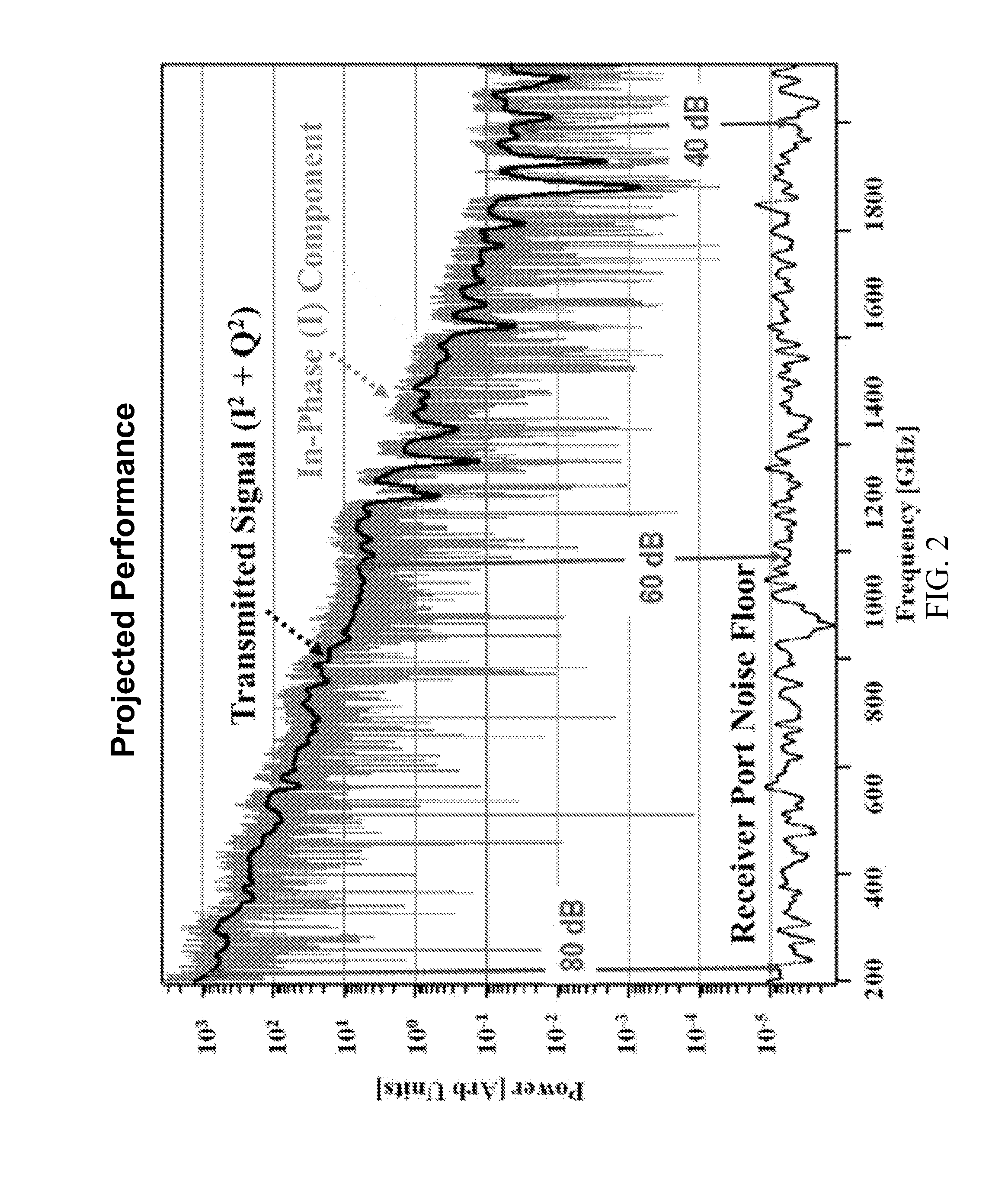
So like all time-domain techniques, the THz power is spread over 1 THz or more, which degrades the instantaneous signal-to-noise ratio considerably compared to a coherent transceiver.
This can be overcome by averaging but then the data acquisition time becomes quite long, on the order of many minutes, which is usually unacceptable for device characterization.

Method used


Image

  • Contact-free photomixing probe for device and integrated circuit measurement or characterization
  • Contact-free photomixing probe for device and integrated circuit measurement or characterization
  • Contact-free photomixing probe for device and integrated circuit measurement or characterization

Examples


Embodiment Construction

[0020]The innovation is now described with reference to the drawings, wherein like reference numerals are used to refer to like elements throughout. In the following description, for purposes of explanation, numerous specific details are set forth in order to provide a thorough understanding of the subject innovation. It may be evident, however, that the innovation can be practiced without these specific details. In other instances, well-known structures and devices are shown in block diagram form in order to facilitate describing the innovation.

[0021]While specific characteristics are described herein (e.g., specific dimensions of example components, etc.), it is to be understood that the features, functions and benefits of the innovation can employ characteristics that vary from those described herein. These alternatives are to be included within the scope of the innovation and claims appended hereto.

[0022]While, for purposes of simplicity of explanation, the one or more methodolo...


PUM

PropertyMeasurementUnit
frequenciesaaaaaaaaaa
heightaaaaaaaaaa
heightaaaaaaaaaa

Abstract

A device for measuring and characterizing solid-state devices or integrated circuits at RF frequencies up to 1.0 THz and beyond is provided that includes a transmitting photomixing probe structure and a receiving photomixing probe structure. The transmitting photomixing probe structure and the receiving photomixing probe structure are ac-coupled to the solid-state device or integrated circuit in a contact-free manner.

Description

CROSS-REFERENCE TO RELATED APPLICATIONS[0001]This application claims the benefit of International Application No. PCT / 2013 / 023633, filed Jan. 29, 2013 which claims the benefit of U.S. Provisional Patent Application Ser. No. 61 / 592,295, entitled “THz PHOTOMIXING PROBE FOR CONTACT-FREE DEVICE AND INTEGRATED CIRCUIT MEASUREMENT OR CHARACTERIZATION,” filed Jan. 30, 2012. The entirety of the above-noted applications are incorporated by reference herein.NOTICE ON GOVERNMENT FUNDING[0002]This innovation was made with government support under a grant awarded by the Office of Naval Research (ONR) Award N00014-11-1-0721. The government has certain rights in the innovation.ORIGIN[0003]The innovation disclosed herein relates to contact-free measurement or characterization of solid-state devices or integrated circuits at RF and THz frequencies, and more specifically, to a contact-free, ac-coupled photomixing probe for use in such measurement or characterization.BACKGROUND[0004]One challenge to t...

Claims


Application Information

Patent Timeline
Patent Type & Authority Applications(United States)
IPC IPC(8): G01N22/00
CPCG01N22/00G01N21/3563G01N21/3581G01R31/311
Inventor BROWN, ELLIOTT R.
Owner WRIGHT STATE UNIVERSITY
Learn More