Stacked wafer structure and fabricating method thereof

Active Publication Date: 2014-12-11
UNITED MICROELECTRONICS CORP
View PDF12 Cites 35 Cited by
  • Summary
  • Abstract
  • Description
  • Claims
  • Application Information

AI Technical Summary

Benefits of technology

[0008]In this regard, methods and structures for assembling the ISP wafer and the CIS wafer a

Problems solved by technology

In a conventional fabricating process, the CIS circuits and ISP circuits are formed on the same substrate, however, results in an increase in the number of processes and high cost.
During the BIS process, the substrate with the ISP circuits has no alternative but to undergo the BI

Method used


Image

  • Stacked wafer structure and fabricating method thereof
  • Stacked wafer structure and fabricating method thereof
  • Stacked wafer structure and fabricating method thereof

Examples


Embodiment Construction

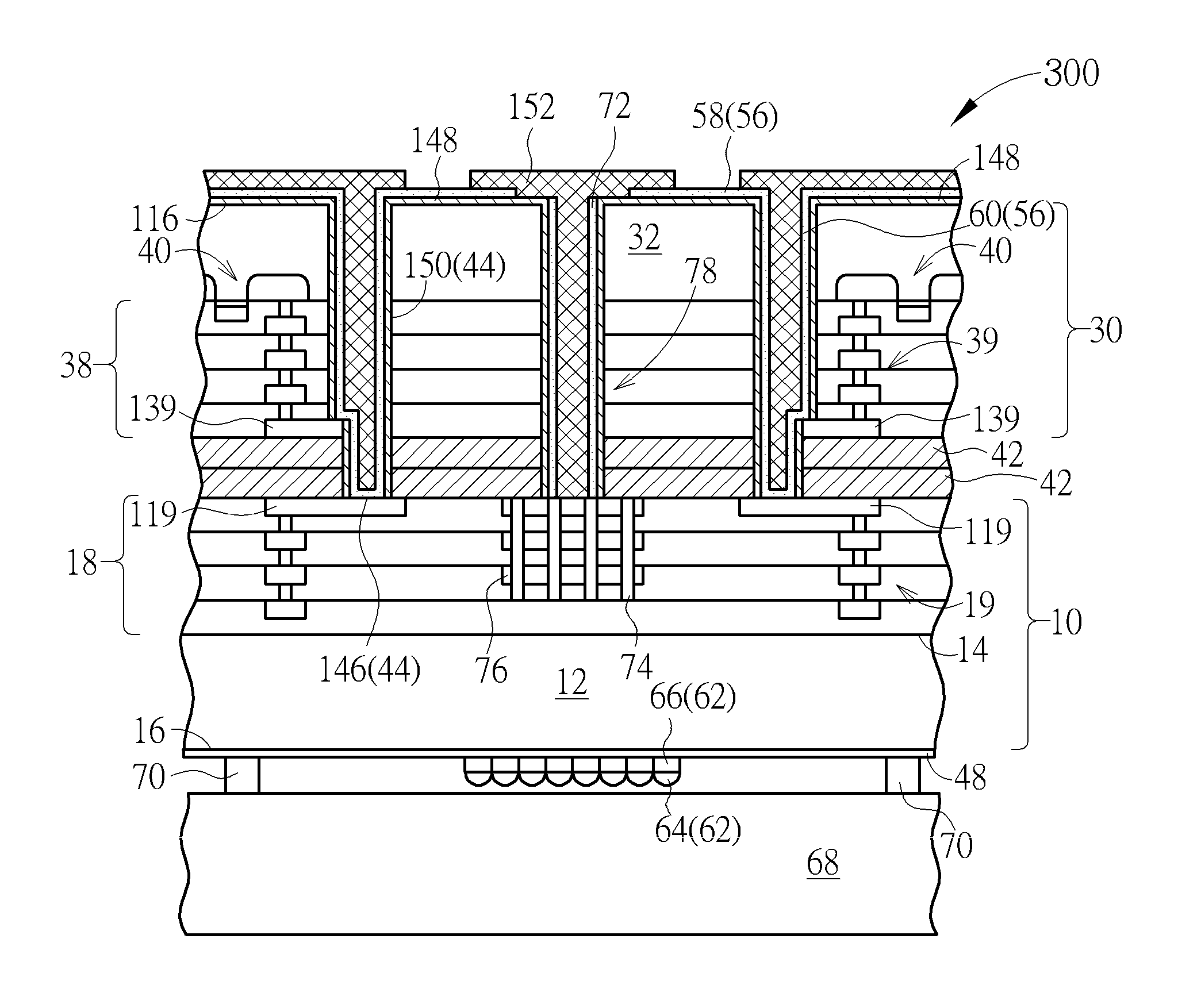
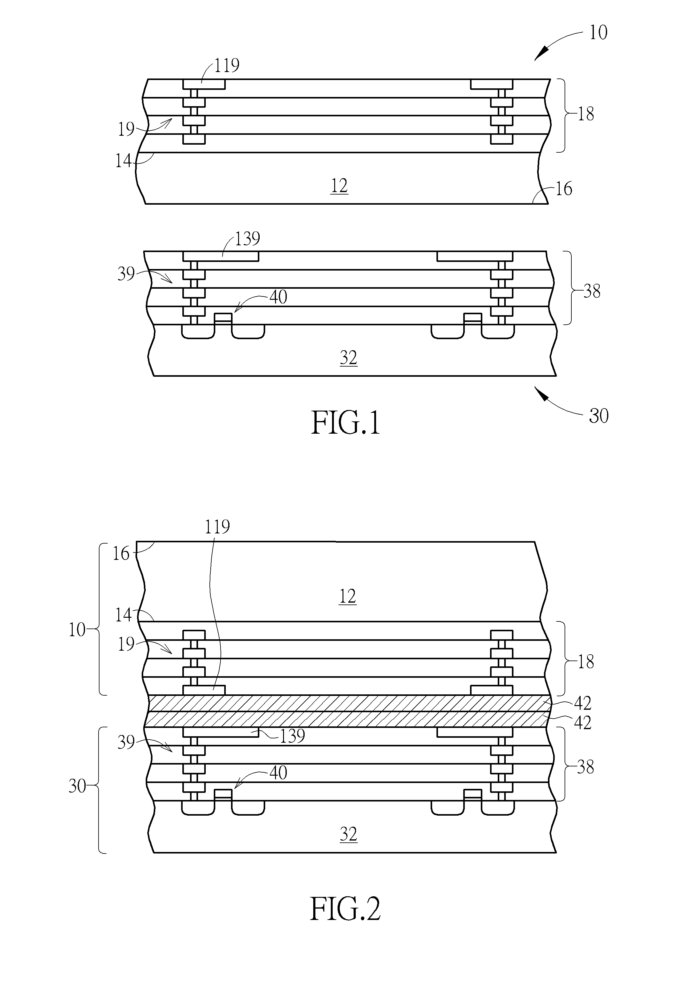
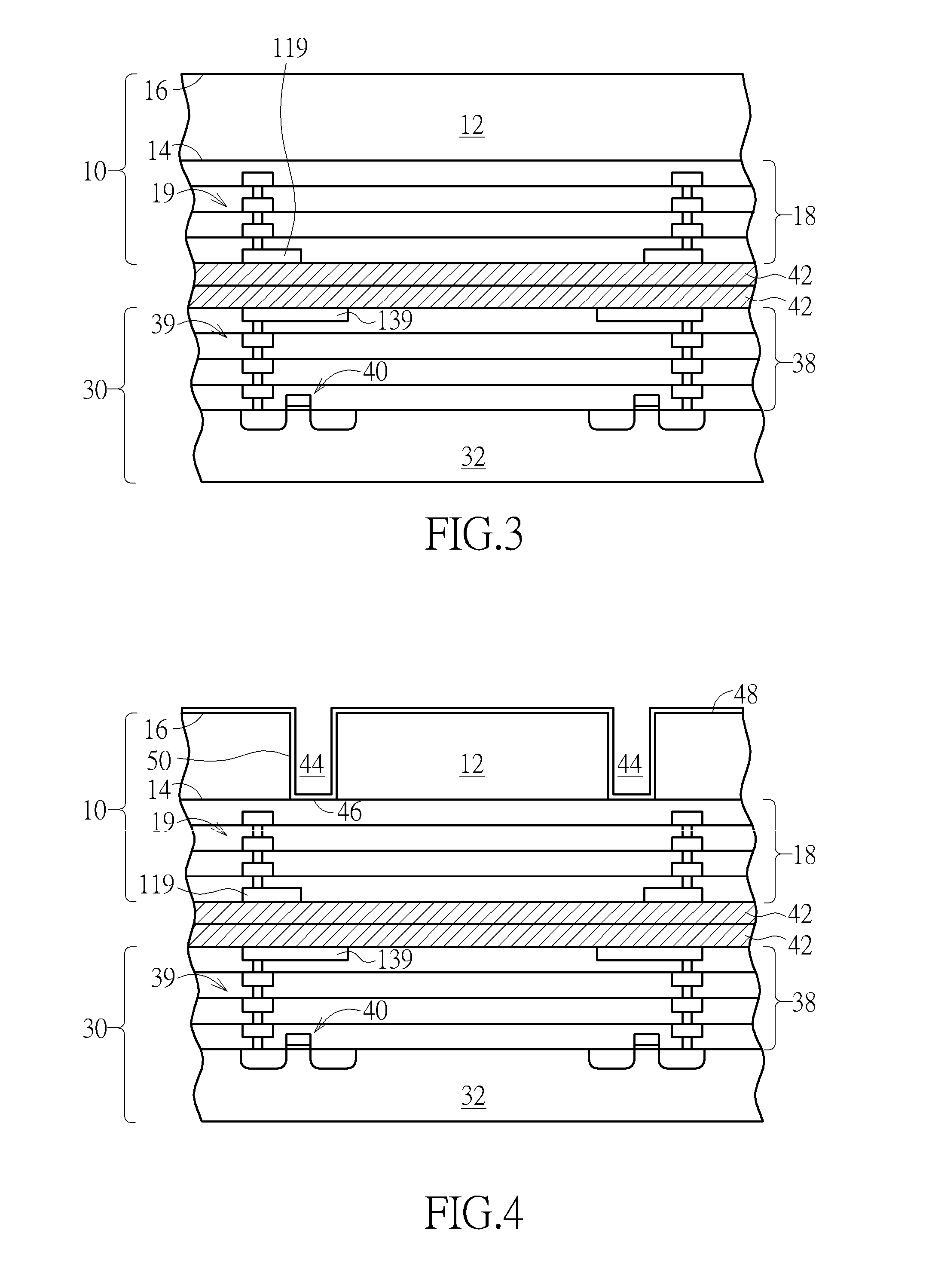
[0016]FIGS. 1 to 7 are schematic cross-sectional diagrams of fabricating a stacked wafer structure at various stages according to a first preferred embodiment of the present invention. It is understood that FIGS. 1 to 7 have been simplified for a better understanding of the inventive concepts of the present disclosure and may not be drawn to scale.

[0017]With reference to FIG. 1, a CMOS image sensors (CIS) wafer 10 and an image signal processor (ISP) wafer 30 are provided. The CIS wafer 10 includes a CIS substrate 12 having a front side 14 and a back side 16, an interlayer dielectric layer 18 disposed on the front side 14 of CIS substrate 12, at least one set of conductive stack 19 disposed within the interlayer dielectric layer 18. The conductive stack 19 may include numerous metal vias and pads. The upmost layer of the conductive stack 19 defined as a last metal 119 which is exposed through the interlayer dielectric layer 18 and often serves as a bonding pad. The front side 14 of t...


PUM


Abstract

A stacked wafer structure includes a CIS wafer, an ISP wafer, a lamination layer, a through silicon via and a pixel device. The CIS wafer bonds to the ISP wafer through the lamination layer. The pixel device is disposed on the CIS wafer. The through silicon via penetrates either the CIS wafer or the ISP wafer to connect devices in CIS wafer to the devices in ISP wafer electrically.

Description

BACKGROUND OF THE INVENTION[0001]1. Field of the Invention[0002]The present invention relates to stacked wafer structure and method of fabricating thereof, and more particularly, to a stacked wafer structure having a trough silicon via penetrate either a CIS wafer or a ISP wafer to electrically connect the device in the CIS wafer to the device in the ISP wafer.[0003]2. Description of the Prior Art[0004]General image sensors are roughly classified into charge coupled device (CCD) image sensors and CMOS image sensors (CISs). Compared with the CCD image sensors, the CISs are widely used in portable apparatuses.[0005]A pixel array of a CIS includes a plurality of pixels, and each of the pixels may generate an image signal from an optical signal. In detail, each of the pixels integrates photocharges corresponding to the amount of light incident using a photodiode and generates an analog pixel signal corresponding to the integrated photocharges.[0006]In general, the analog pixel signal ou...

Claims


Application Information

Patent Timeline
IPC IPC(8): H01L27/148H01L27/146
CPCH01L27/14687H01L27/14812H01L27/14627H01L27/1463H01L27/14634H01L27/14636H01L27/1469H01L23/481H01L21/76898
Inventor KAO, CHING-HUNG
Owner UNITED MICROELECTRONICS CORP
Why Eureka
Try Eureka