Semiconductor structure and method of forming a harmonic-effect-suppression structure

a semiconductor structure and harmonic effect technology, applied in the field of semiconductor structure for suppressing harmonic effects, can solve problems such as performance suffers, and achieve the effect of suppressing harmonic effects and avoiding parasitic surface charges

Active Publication Date: 2015-01-01
UNITED MICROELECTRONICS CORP
View PDF1 Cites 4 Cited by
  • Summary
  • Abstract
  • Description
  • Claims
  • Application Information

AI Technical Summary

Benefits of technology

[0009]In the present invention, the silicon layer can function as a charge release layer or a trap layer to freeze charges generated at the interface of the buried dielectric and the base semiconductor substrate. In other words, the charges can be attracted or trapped by t

Problems solved by technology

In radio frequency (RF) integrated circuit application, such as RF switch device or power amplifier device, performance is suffered from “parasitic surface charge” issue,

Method used


Image

  • Semiconductor structure and method of forming a harmonic-effect-suppression structure
  • Semiconductor structure and method of forming a harmonic-effect-suppression structure
  • Semiconductor structure and method of forming a harmonic-effect-suppression structure

Examples


Embodiment Construction

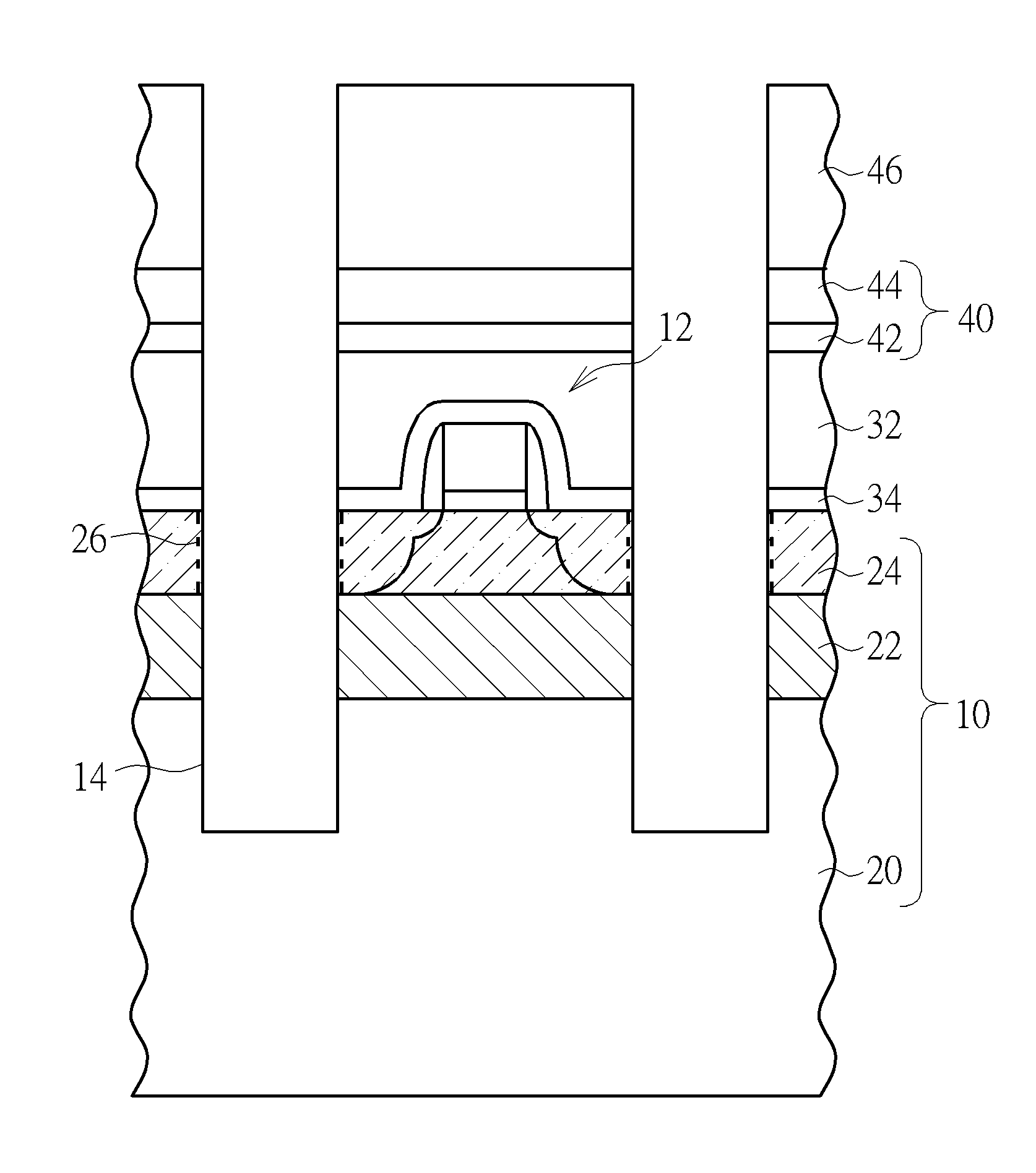
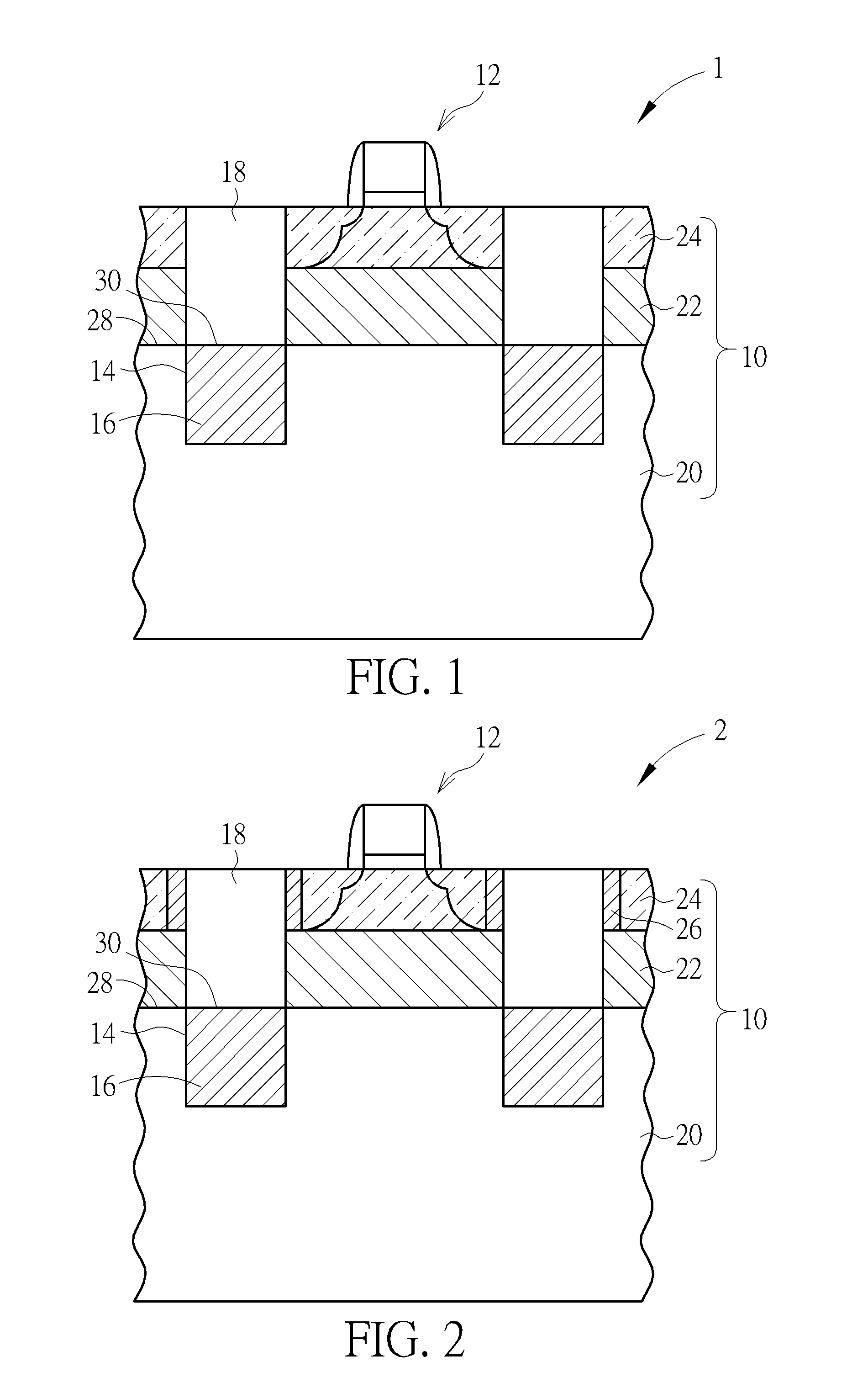
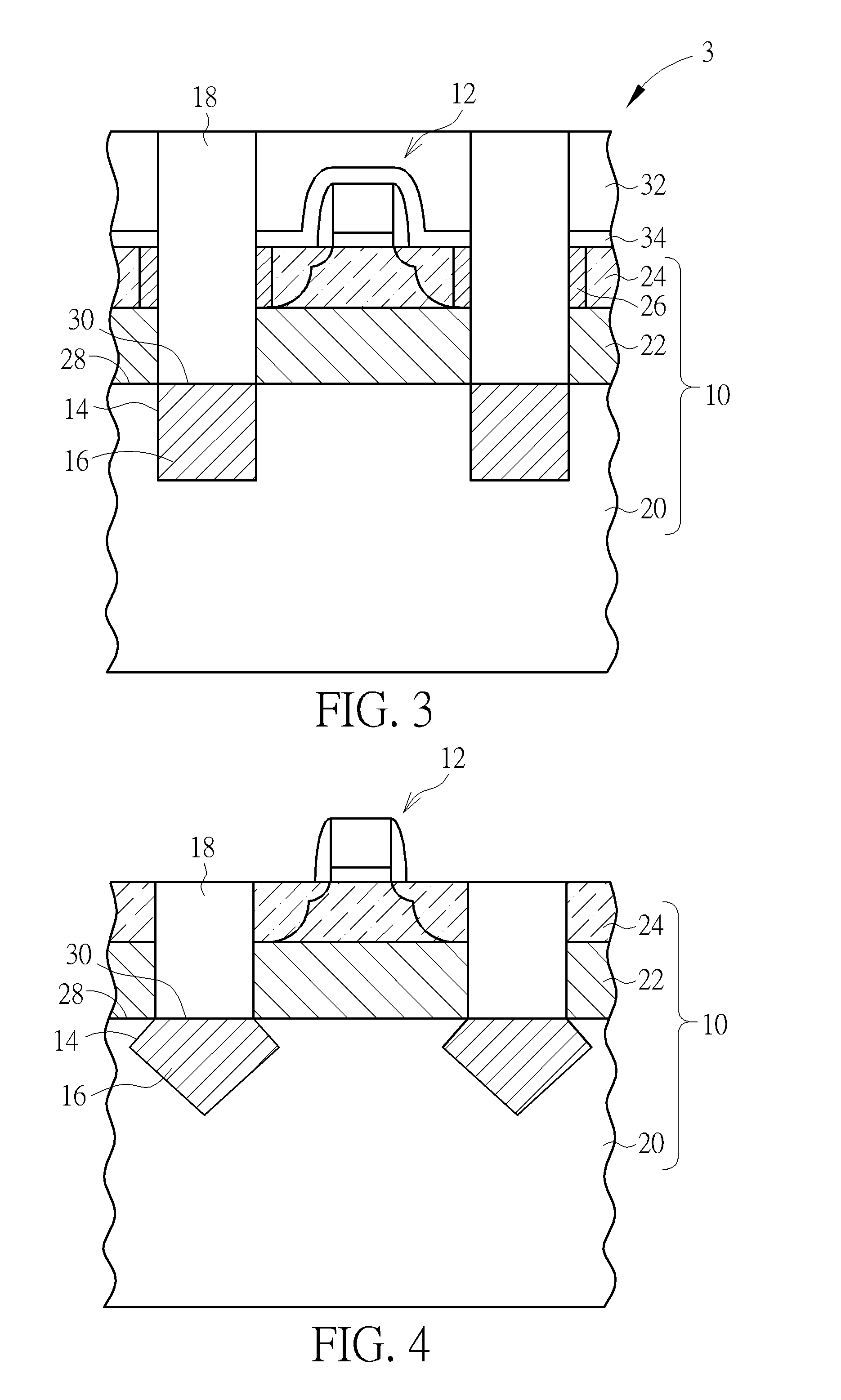
[0016]FIGS. 1 to 5 are cross-sectional views illustrating some semiconductor structures of some embodiments according to some aspects of the present invention. Referring to FIG. 1, the semiconductor structure 1 according to an embodiment of the present invention includes a semiconductor substrate 10, a device 12, a deep trench 14, a silicon layer 16 and a dielectric layer 18. The semiconductor substrate 10 includes a base semiconductor substrate 20, a buried dielectric 22 disposed on the base semiconductor substrate 20, a surface semiconductor layer 24 disposed on the buried dielectric 22, and a shallow trench isolation layer 26 disposed in the surface semiconductor layer 24. The base semiconductor substrate 20 may include, for example, a silicon material of high resistivity, such as an amorphous silicon layer, or a silicon substrate including SiGe layer, but not limited thereto. The buried dielectric 22 may include, for example, oxide layer. The buried oxide in this technical field...


PUM


Abstract

A semiconductor structure includes a SOI/BOX semiconductor substrate, a device, a deep trench, a silicon layer, and a dielectric layer. The deep trench is adjacent to the device and extends through a shallow trench isolation layer within the SOI layer and the BOX layer and into the base semiconductor substrate. The silicon layer is disposed within a lower portion of the deep trench. The silicon layer has a top surface height substantially the same as or lower than a top surface height of the base semiconductor substrate. The dielectric layer is disposed within the deep trench and on the silicon layer. The deep trench can be formed before or after formation of an interlayer dielectric.

Description

BACKGROUND OF THE INVENTION[0001]1. Field of the Invention[0002]The present invention relates to a semiconductor technology, and particularly to a technology for harmonic effect suppression in a semiconductor structure.[0003]2. Description of the Prior Art[0004]In radio frequency (RF) integrated circuit application, such as RF switch device or power amplifier device, performance is suffered from “parasitic surface charge” issue, which in turn generates harmonic effect. There are several wafer process technologies available for solving the issue such as using semiconductor-on-insulator (SOI) wafer to isolate the charges from the high resistivity wafer substrate. However, as the RF switch goes high frequency, it is more sensitive to RF harmonic effect induced by the parasitic surface charges. The problem needs to be solved.SUMMARY OF THE INVENTION[0005]One objective of the present invention is to provide a semiconductor structure and a method of forming a harmonic-effect-suppression s...

Claims


Application Information

Patent Timeline
IPC IPC(8): H01L21/762H01L29/06
CPCH01L29/0649H01L21/76224H01L21/02532H01L21/02595H01L21/02664H01L21/26506H01L21/30604H01L21/30625H01L21/3081H01L21/76232H01L21/7624H01L21/76283H01L21/76898
Inventor CHEN, TONG-YUYANG, KUO-YUH
Owner UNITED MICROELECTRONICS CORP
Why Eureka
Try Eureka