Active pixel structure with improved charge transfer

a charge transfer and active pixel technology, applied in the field of cmos integration technology, can solve the problems of inability to compensate, and low switching noise ktc, and achieve the effect of reducing the noise of readout, pixel afterglow, and low charge-voltage conversion factor

Active Publication Date: 2015-01-08
NEW IMAGING TECH
View PDF6 Cites 10 Cited by
  • Summary
  • Abstract
  • Description
  • Claims
  • Application Information

AI Technical Summary

Benefits of technology

[0053]In this manner, it is no longer necessary to obtain precise alignment between the gate of the transfer transistor and the photodiode. The gate of the transfer transistor can be deposited after forming the photodiode, and it is therefo

Problems solved by technology

However the charge-voltage conversion factor is low on account of the strong value of the junction capacitor forming the photodiode.
In addition, during reset readout after time t3, there occurs a switching noise KTC perturbing proper readout of the initial voltage and which cannot be compensated.
Incomplete charge transfer creates readout noise and pixel afterglow.
An energy pocket may retain part of the charges during transfer and will cause the same problems of noise and pixel afterglow.
In addition, in this structure of a four-transistor pixel the coupling between the photoelectric conversion zone NPD and the gate of the transfer transistor TX fo

Method used


Image

  • Active pixel structure with improved charge transfer
  • Active pixel structure with improved charge transfer
  • Active pixel structure with improved charge transfer

Examples


first embodiment

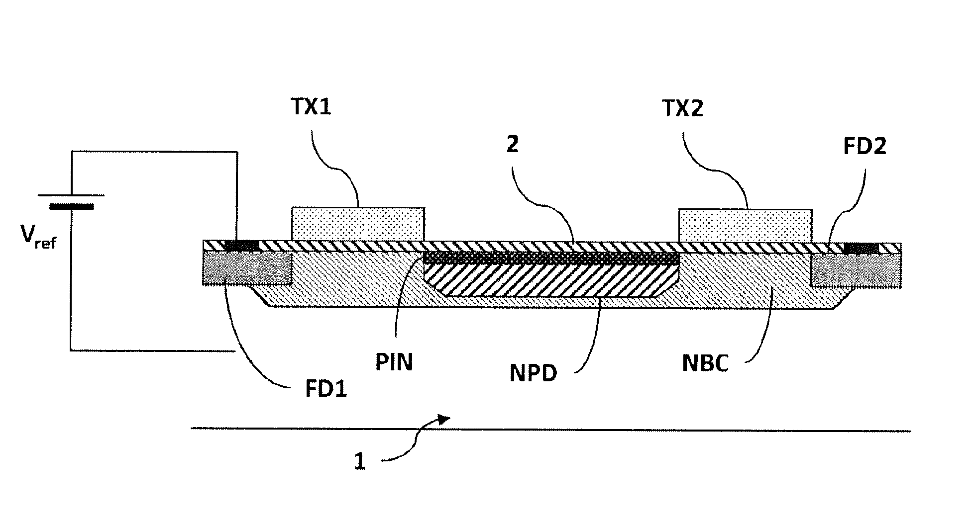
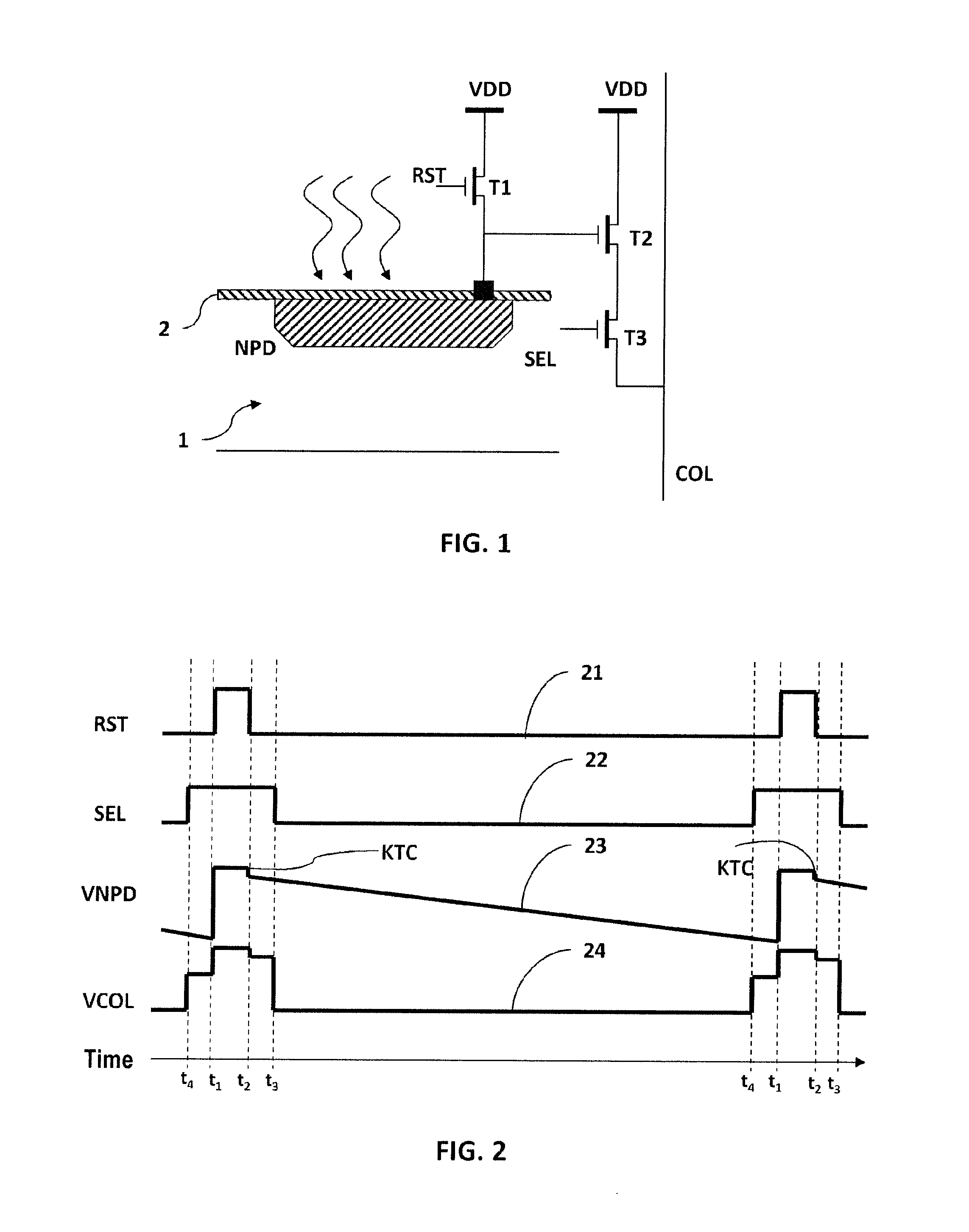
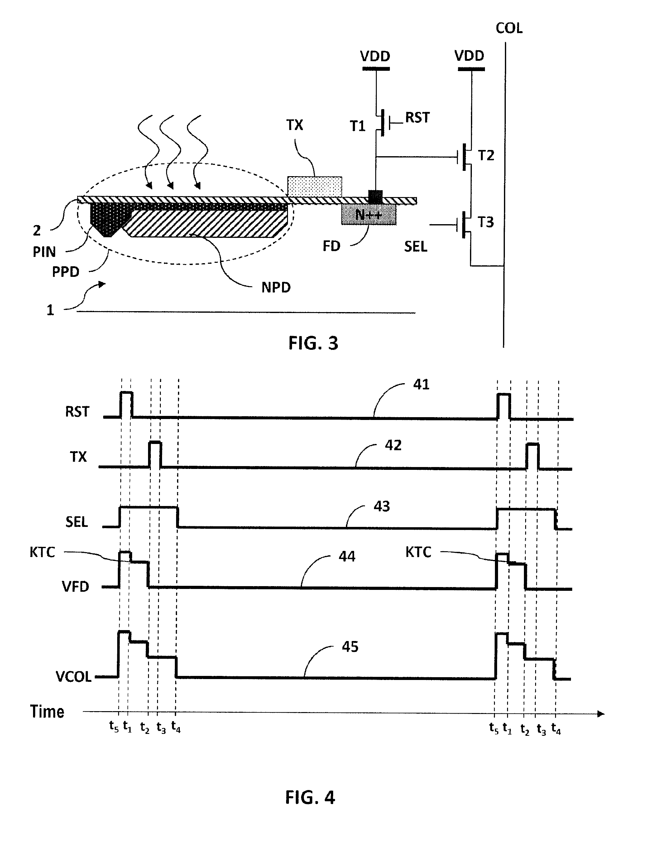
[0097]With reference to FIG. 8, an active pixel structure comprises a P-type semiconductor substrate 1 in which at least one photoelectric conversion zone NPD is defined by N-type doping to accumulate an amount of charge during exposure to light. A shallow, heavily P-doped surface zone PIN forms a co-called “pinning” layer for ground pinning of the surface potential of the photoelectric conversion zone NPD.

[0098]A floating diffusion node FD defined by N-doping in the substrate 1 is arranged at a distance away from the photoelectric conversion zone NPD. The N-doping of the floating diffusion node FD is generally heavier than the N-doping of the photoelectric conversion zone NPD.

[0099]Very often the floating diffusion node FD can be merged with the source of the reset transistor T1.

[0100]An isolating layer 2 of silicon dioxide is arranged on the surface of the substrate 1 and in particular insulates the gate of the transfer transistor TX from the substrate 1.

[0101]The structure furth...

second embodiment

[0152]With this second embodiment it is possible to place the main forming of the photodiode PPD before the fabrication steps of the CMOS transistors, and thereby achieve considerable relaxation of heat budget constraints between the needs of the photodiode and those of the CMOS transistors.

[0153]FIGS. 15a and 15b illustrate examples of a pixel structure according to the second embodiment.

[0154]As in the first embodiment, the active pixel structure of CMOS type comprises:[0155]a P-type semiconductor substrate;[0156]at least one photoelectric conversion zone NPD defined by N-doping in the substrate, accumulating an amount of charge during exposure to light and comprising a P-doped surface zone PIN;[0157]at least one floating diffusion node FD defined by N-doping in the substrate;[0158]at least one readout circuit to read a variation in voltage on the floating diffusion node FD induced by the transferred charges;[0159]at least one transfer transistor TX of MOS type, the gate of said t...


PUM


Abstract

The invention relates to an active CMOS pixel structure comprising: at least one photoelectric conversion zone (NPD) defined by n-doping of the substrate, said zone accumulating an amount of charge during an exposure to light and comprising a p-doped surface zone (PIN); and at least one MOS transfer transistor (TX), the gate of said transfer transistor (TX) being electrically insulated from the substrate and being used to control transfer of said charge from said photoelectric conversion zone (NPD) to said floating diffusion node (FD), in which the gate of said transfer transistor (TX) partially covers said p-doped surface zone (PIN), and said photoelectric conversion zone (NPD) extends under said gate of said transfer transistor (TX) at least as far as the end of the p-doped surface zone (PIN).

Description

GENERAL TECHNICAL FIELD AND BACKGROUND OF THE INVENTION[0001]The invention concerns CMOS integration technology (Complementary Metal Oxide Semiconductor) using a family of electronic components with low electric consumption. The invention particularly concerns CMOS pixel structures and image sensor arrays incorporating the same.[0002]CMOS integration technology allows the production of chips for monolithic cameras having good resolution and reasonable image quality. The application of these techniques also allows the obtaining of sensors with low energy consumption. Such sensors also offer fast reading speed on account of the very good operating dynamics of CMOS pixels through the rapid switching of CMOS transistors. In addition, these technologies offer the possibility of integrating packaging, processing, coding and communication functions.[0003]FIG. 1 illustrates the structure of a pixel of an active pixel sensor (APS) having three transistors. Said pixel comprises:[0004]a P-type...

Claims


Application Information

Patent Timeline
IPC IPC(8): H01L27/146
CPCH01L27/14689H01L27/14616H01L27/14643H01L27/14612H01L27/1463
Inventor NI, YANG
Owner NEW IMAGING TECH
Why Eureka
Try Eureka