Method For Detecting Buried Layers

a technology of optical detection and buried layers, applied in the direction of material testing goods, instruments, testing semiconductor materials, etc., can solve the problems of high accuracy, high accuracy, and inability to meet the requirements of high throughput, and achieve high speed

Inactive Publication Date: 2015-01-15
HSEB DRESDEN
View PDF5 Cites 6 Cited by
  • Summary
  • Abstract
  • Description
  • Claims
  • Application Information

AI Technical Summary

Benefits of technology

[0011]It is an object of the invention to provide an assembly of the above mentioned kind which operates destruction-f

Problems solved by technology

Ellipsometric measurements are highly sensitive but only work point-wise.
The ellipsometric measuring procedure requires considerable measuring time for each inspected point, because usually mechanical parts, such as the analyzer, must be moved.
Ellipsome

Method used


Image

  • Method For Detecting Buried Layers
  • Method For Detecting Buried Layers
  • Method For Detecting Buried Layers

Examples


Embodiment Construction

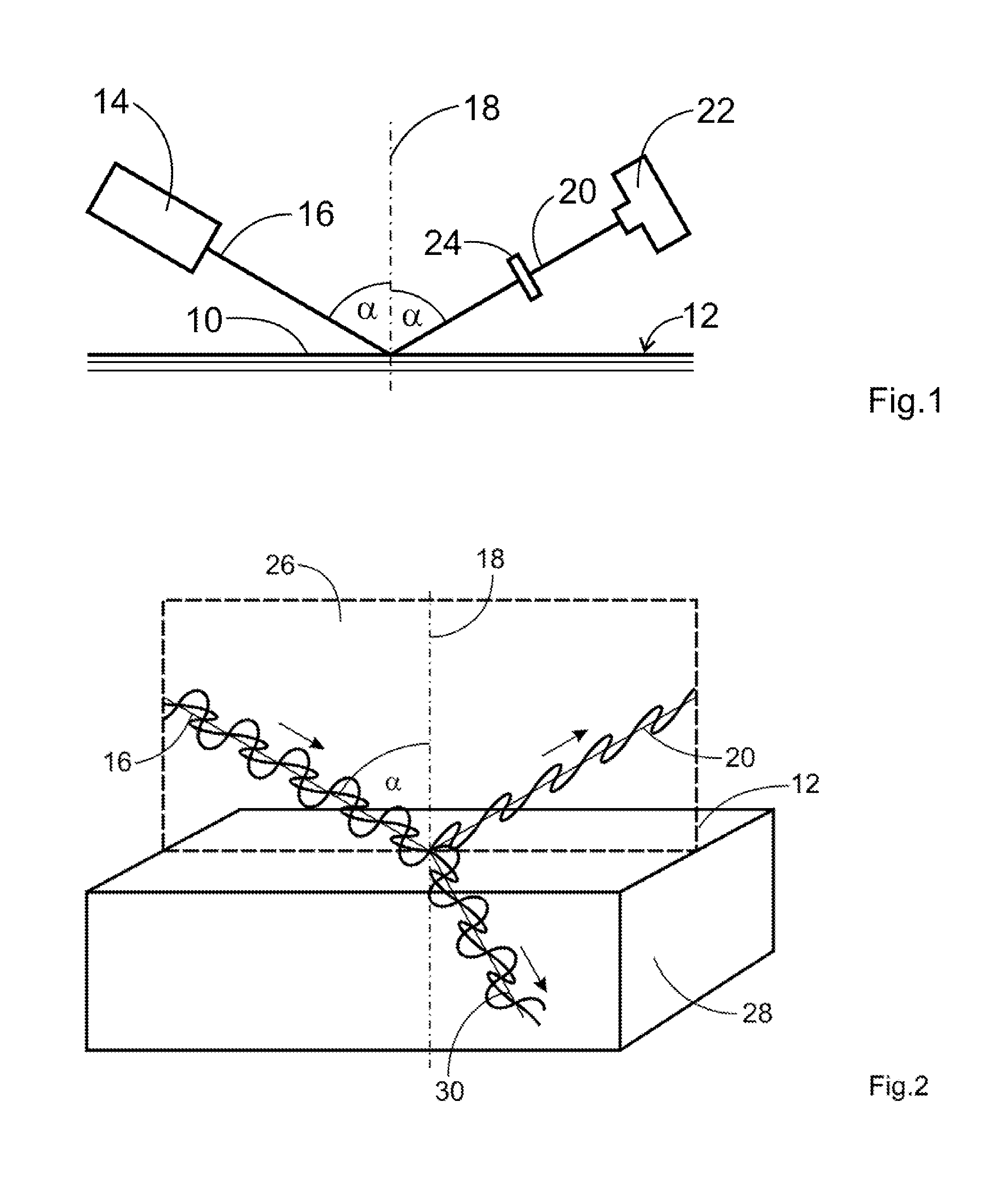
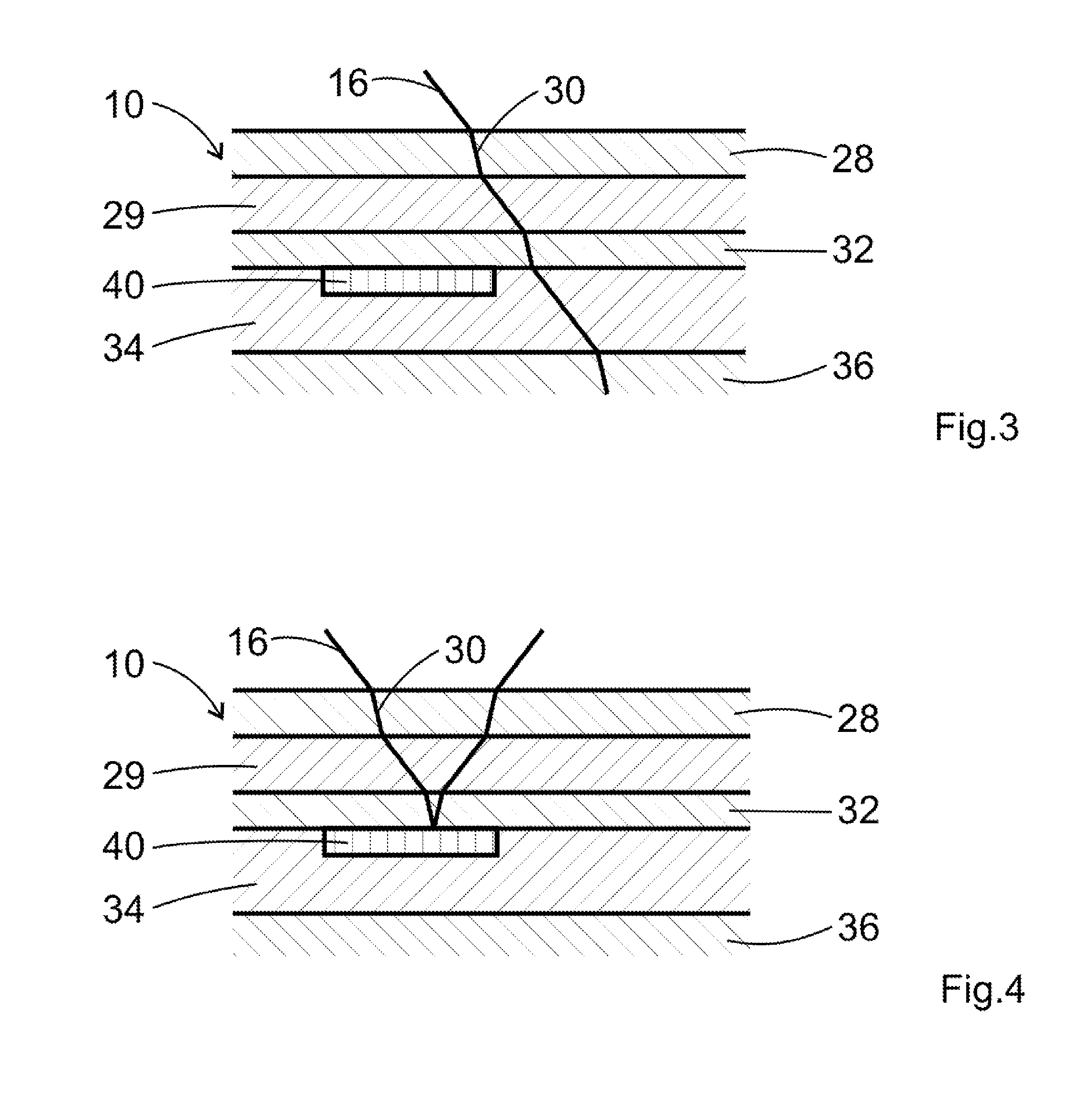
[0038]FIG. 1 shows an object generally designated with numeral 10. In the present embodiment the object 10 is a wafer with a silicon substrate 28, 32, and 36 having several vertically stacked, air-filled spaces 29 and 34. The spaces 29 and 34 are separated from each other by small layers 32 and 36 of silicon as can be seen in FIGS. 3 and 4. Due to production conditions in some of the spaces 29 and 34 defects can occur in the form of silicon oxide layers 40. This corresponds to the negative check.

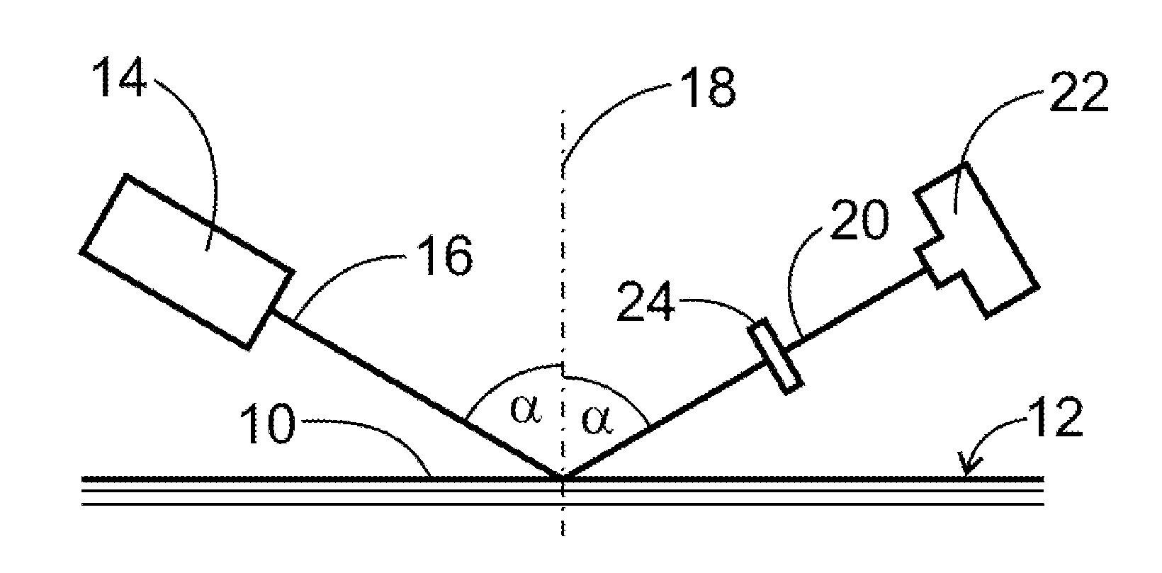
[0039]Each of the materials, i.e. silicon, silicon oxide and air are defined by their refractive index nx. The refractive index of the uppermost layer 28 of silicon is 3.5. The refractive index of the air layer 29 therebelow is 1.0. FIG. 1 schematically illustrates the measuring assembly. The surface 12 of the object is illuminated with infrared radiation 16 from an infrared radiation source 14, In the present embodiment broad band radiation from the wavelength range between 1.1 microns and ...


PUM


Abstract

An arrangement for optically detecting buried layers of flat objects having a plurality of layers, in particular wafers, containing a radiation source for illuminating the surface of the object at an angle; a polarization filter arranged in the beam path; and a detector for detecting radiation reflected by the surface of the object or transmitted by the object; is characterized in that that layer of the object which is closest to the radiation source at least partially transmits the radiation from the radiation source; the polarization filter transmits only radiation which is polarized parallel to the plane of incidence; and the surface of the object is illuminated at the Brewster angle. The surface of the object is preferably illuminated with unpolarized radiation and the polarization filter is arranged in the beam path between the surface of the object and the detector.

Description

TECHNICAL FIELD[0001]The invention relates to an assembly for optical detection of buried layers of flat objects with a plurality of layers, in particular wafers, comprising:[0002](a) a radiation source for illuminating the surface of the object;[0003](b) a polarization filter arranged in the path of rays; and[0004](c) a detector for the detection of radiation reflected by the surface of the object or transmitted by the object.[0005]In different industry branches, flat products and their properties are inspected with optical. imaging methods. In the semiconductor and flat panel industry these flat products are, amongst others, wafers. Wafers are discs made of semiconductor-, glass-, sheet- or ceramic materials. In various processing steps during manufacturing, different materials are arranged on top of each other and thereby stacks with layers are produced.[0006]Exact knowledge of the generated layers is required for production control and quality management. For different reasons, ...

Claims


Application Information

Patent Timeline
IPC IPC(8): G01N21/55G01N33/00
CPCG01N33/00G01N2201/068G01N2033/0095G01N21/55G01N21/8422G01N21/9505G01N2021/8438
Inventor SROCKA, BERNDLANGHANS, RALF
Owner HSEB DRESDEN
Why Eureka
Try Eureka