
Super junction mosfet, method of manufacturing the same, and complex semiconductor device

a technology of super junction mosfet and vertical mosfet, which is applied in the direction of semiconductor devices, diodes, electrical apparatuses, etc., can solve problems such as noise generation, and achieve the effects of low reverse recovery loss, low reverse recovery current irp and reverse recovery time trr, and high speed switching

Active Publication Date: 2015-01-15
FUJI ELECTRIC CO LTD
View PDF1 Cites 7 Cited by
  • Summary
  • Abstract
  • Description
  • Claims
  • Application Information

AI Technical Summary

Benefits of technology

The invention is a type of MOSFET that can switch quickly and has low loss when recovering from previous use. This is achieved by relaxing the way it recovers, which reduces the amount of electric current that needs to be recovered and the time it takes to recover. The invention can be used in complex semiconductor devices to improve their performance.

Problems solved by technology

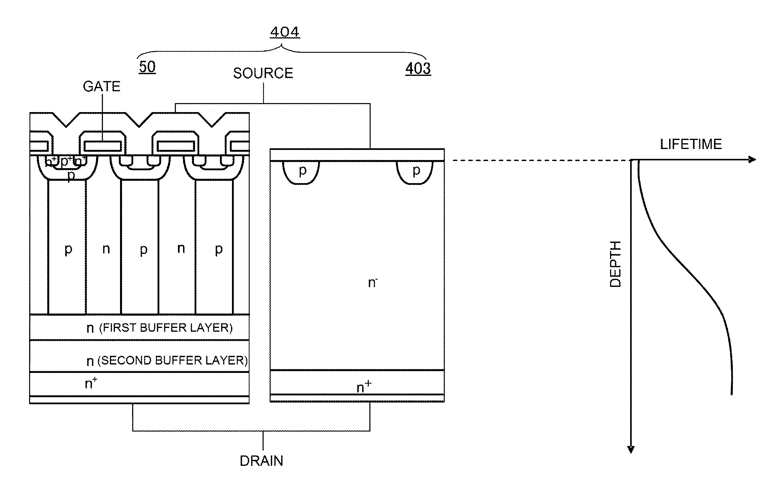
When a reverse recovery operation forms a hard recovery waveform, the problem is that ringing occurs (an oscillatory waveform is formed), thus causing noise generation, as shown in a reverse recovery waveform diagram of the heretofore known super junction MOSFET of FIG. 4 (in FIG. 4, the oscillatory waveform portions are overlapped in a blacked out condition and difficult to see).

Method used


Image

  • Super junction mosfet, method of manufacturing the same, and complex semiconductor device
  • Super junction mosfet, method of manufacturing the same, and complex semiconductor device
  • Super junction mosfet, method of manufacturing the same, and complex semiconductor device

Examples


first embodiment

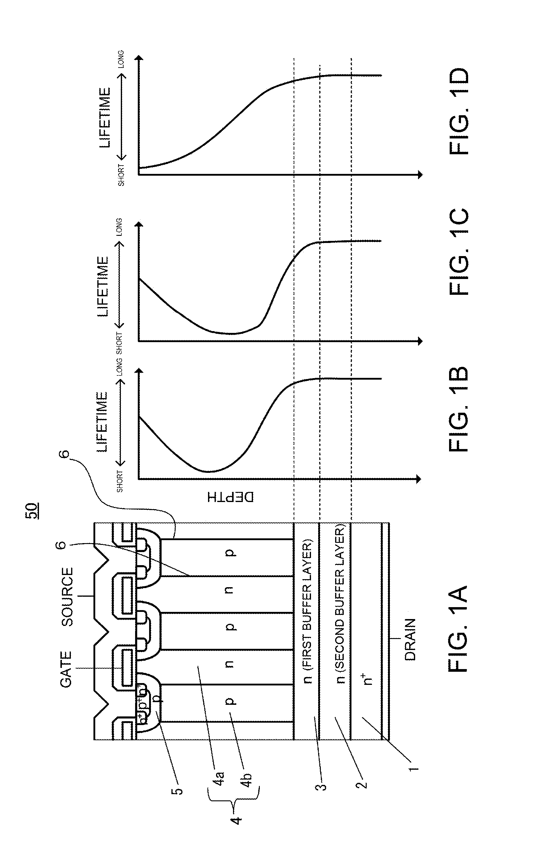
[0024]FIG. 1A shows a main portion sectional view of an element active portion of a vertical super junction MOSFET according to the invention. FIGS. 1B, 1C, and 1D are carrier lifetime distribution charts with the depth of the super junction MOSFET shown in FIG. 1A related to the vertical axis and the lifetime thereof on the horizontal axis, and although the depth ranges of the respective lifetime-controlled regions are different from each other, are all of the preferred super junction MOSFET according to the invention.

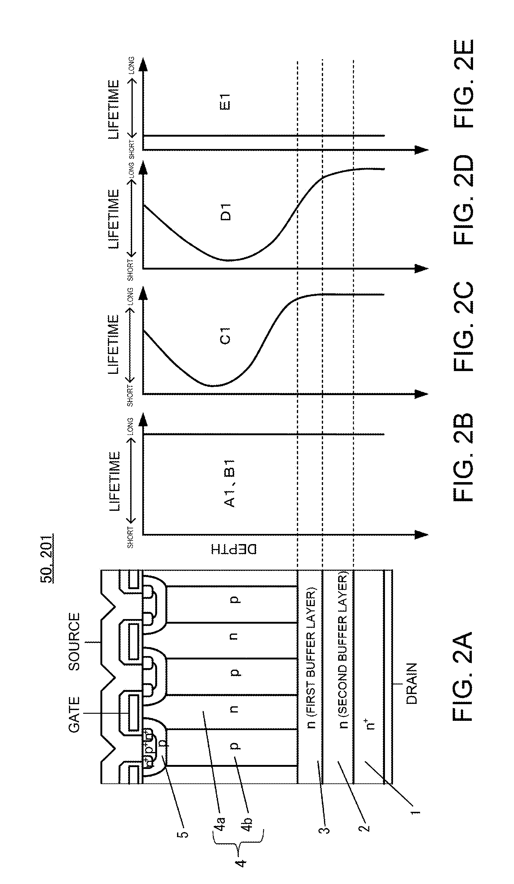
[0025]The super junction MOSFET includes an n-type second buffer layer 2 of a higher concentration than an n-type drift region 4a, and an n-type first buffer layer 3 of a concentration equal to or lower than the drift region 4a, on an n+-type semiconductor substrate (n+drain layer 1) of a high concentration, and includes a parallel pn layer 4 on the n-type first buffer layer 3. The pattern of a cross section of the parallel pn layer 4 taken along a plane parallel to t...


PUM

PropertyMeasurementUnit
forward currentaaaaaaaaaa
supply voltageaaaaaaaaaa
breakdown voltageaaaaaaaaaa

Abstract

A super junction MOSFET is disclosed. The super junction MOSFET includes a plurality of mutually parallel pn junctions extending in a vertical direction on a first principal surface of an n-type semiconductor substrate; a parallel pn layer in which n-type drift regions and p-type partition regions, each sandwiched between the adjacent pn junctions, are disposed alternately in contact with each other; and an MOS gate structure on the first principal surface side of the parallel pn layer, wherein an n-type first buffer layer and second buffer layer are in contact in that order on the opposite principal surface side, and the impurity concentration of the first buffer layer is a concentration that is equal to or less than the same level as that of the impurity concentration of the n-type drift region.

Description

CROSS REFERENCE TO RELATED APPLICATION[0001]The entire disclosure of the inventor's corresponding Japanese patent application, Serial No. JP PA 2013-144654, filed Jul. 10, 2013, is hereby incorporated by reference.BACKGROUND OF THE INVENTION[0002]1. Field of the Invention[0003]The present invention relates to a vertical MOSFET (insulated gate field effect transistor), a method of manufacturing the vertical MOSFET, and a complex semiconductor device.[0004]2. Description of the Background Art[0005]As a high breakdown voltage switching element used for an inverter circuit 1000 shown in FIG. 6, an IGBT 101 is widely used. The IGBT 101, having features of a bipolar transistor, such as a high breakdown voltage and a low on voltage, and the superior feature of being able to operate at high speed although being lower in speed than an MOSFET, is an important semiconductor element which underpins the present power electronics.[0006]However, the IGBT 101 shown in a main portion sectional view ...

Claims


Application Information

Patent Timeline
Patent Type & Authority Applications(United States)
IPC IPC(8): H01L29/78H01L21/26H01L29/66H01L29/06H01L29/10
CPCH01L29/1095H01L29/0634H01L29/7806H01L21/26H01L29/7804H01L29/66712H01L29/7802H01L29/7805H01L29/0878
Inventor TAMURA, TAKAHIROONISHI
Owner FUJI ELECTRIC CO LTD
Learn More