Nitride semiconductor device and method for producing nitride semiconductor device

a technology of nitride and semiconductors, applied in the direction of semiconductor devices, basic electric elements, electrical apparatus, etc., can solve the problems of large number of dislocation defects, and possible generation of crystal defects, etc., and achieve excellent power devices and reduce the threshold voltage

Inactive Publication Date: 2008-08-28
ROHM CO LTD
View PDF4 Cites 15 Cited by
  • Summary
  • Abstract
  • Description
  • Claims
  • Application Information

AI Technical Summary

Benefits of technology

[0017]Accordingly, during operation of the above-described MISFET, a region in which the inversion layer (channel) is formed is the fourth layer. As a result, when the fourth layer is a p-type semiconductor having a lower acceptor concentration than that of the second layer, for example, it is possible to keep a gate threshold voltage required for forming the inversion layer to a lower level, as compared to a case where a conductive characteristic of the region in which the inversion layer is formed is the same as that of the second layer. Therefore, the gate threshold...

Problems solved by technology

However, at steps of manufacturing the above-mentioned vertically structured GaN device, resulting from a mismatch between a lattice constant of the SiC substrate and that of the GaN thin film, a large number of dislocation defects (crystal defects) which penetrate in a perpendicular direction from the SiC substrate through the GaN thin film and the n-type GaN layer may possibly be...

Method used


Image

  • Nitride semiconductor device and method for producing nitride semiconductor device
  • Nitride semiconductor device and method for producing nitride semiconductor device
  • Nitride semiconductor device and method for producing nitride semiconductor device

Examples


first embodiment

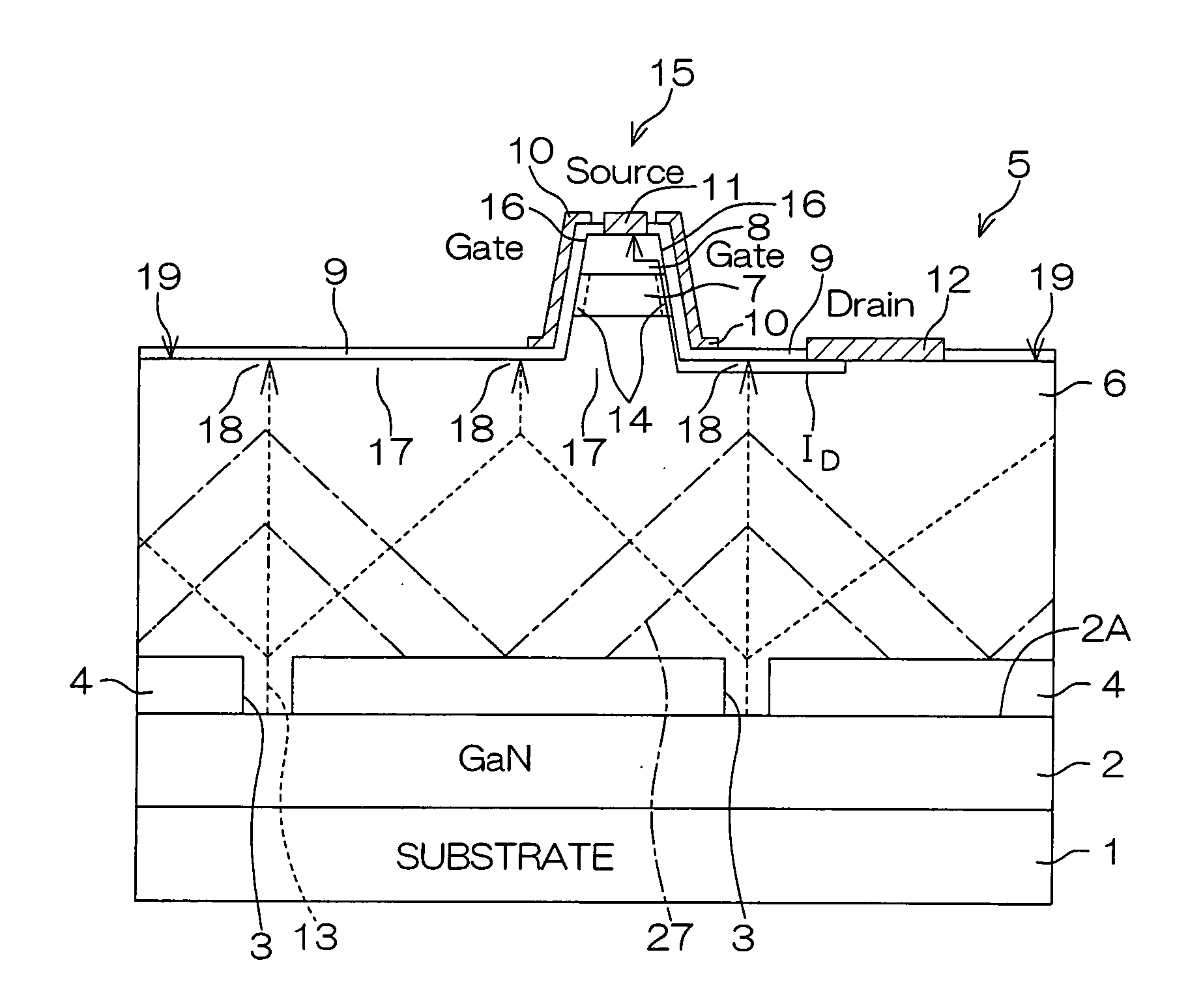
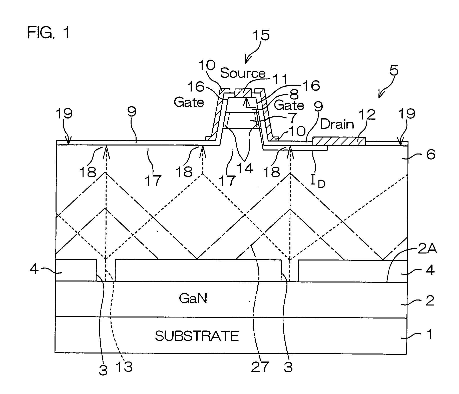
[0051]FIG. 1 is a diagrammatic cross-sectional view for describing a structure of a field effect transistor according to the present invention.

[0052]The field effect transistor is provided with: a substrate 1 (base layer); a GaN film 2 (base layer, conductive base layer) grown on the substrate 1; an insulating film mask 4 (insulating film) which is formed on a main surface 2A of the GaN film 2 and has an opening 3 for exposing a part of the main surface 2A; and a nitride semiconductor laminated structure 5 (nitride semiconductor structure) formed in a region from the opening 3 of the insulating film mask 4 to an upper area of the insulating film mask 4.

[0053]For the substrate 1, an insulative substrate such as a sapphire substrate or the like, or a conductive substrate such as a GaN substrate, a ZnO substrate, Si substrate, a GaAs substrate, SiC substrate or the like, may be applied, for example.

[0054]The GaN film 2 is one example of a Group III nitride semiconductor compound expres...

second embodiment

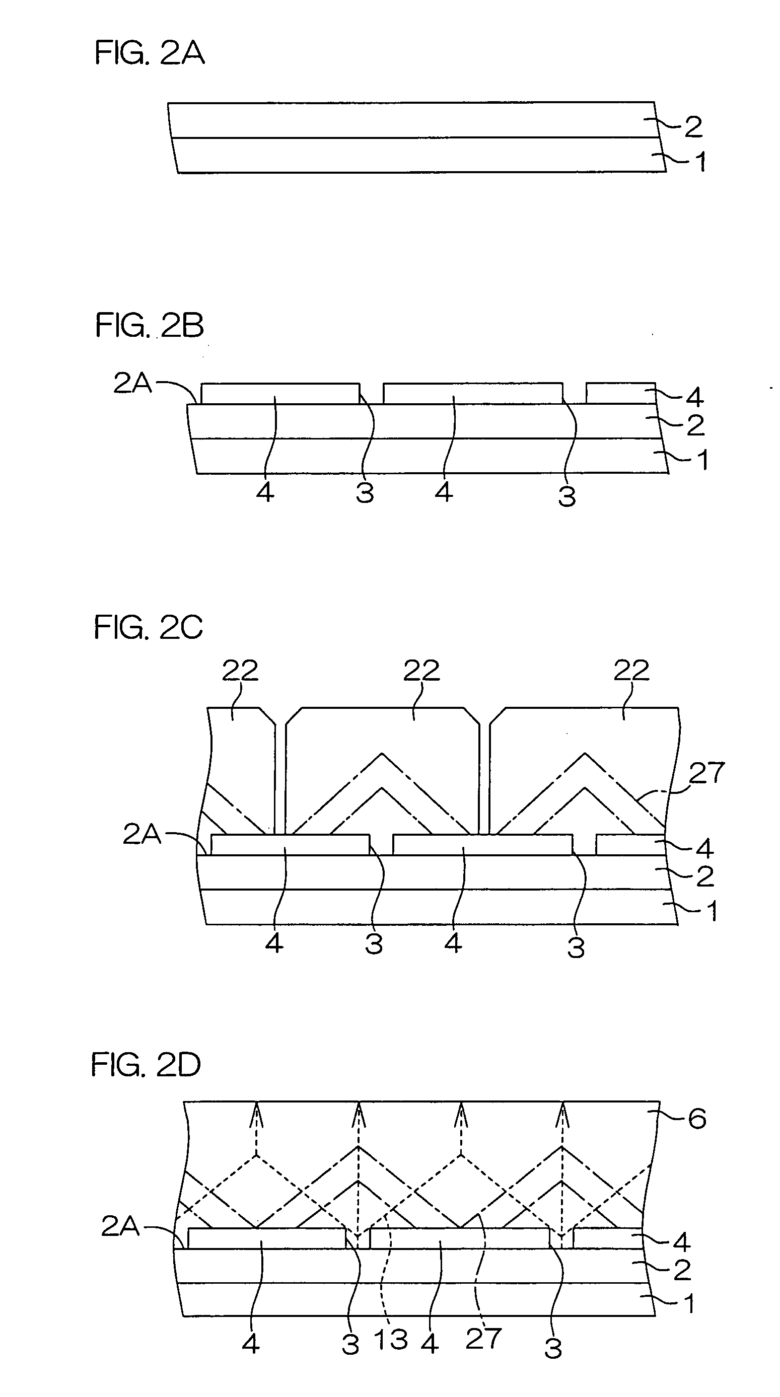
[0089]FIG. 3 is a diagrammatic cross-sectional view for describing a structure of a field effect transistor according to the present invention. In FIG. 3, parts corresponding to those in the preceding FIG. 1 are designated by the same reference numerals as those in FIG. 1.

[0090]In this embodiment, no insulating film mask 4 is formed on the main surface 2A of the GaN film 2, and the GaN film 2 is formed with a depression 23 by etching to a certain film thickness of the GaN film 2 from the main surface 2A. The depression 23 is formed to form protrusions 21 higher by a step level than the depression 23 on both sides of the depression 23 in the GaN film 2.

[0091]The nitride semiconductor laminated structure 5 is formed on a region which extends from the depression 23 to upper areas of the protrusions 21, i.e., an entire surface of the GaN film 2. In the interior of the nitride semiconductor laminated structure 5 (interior of the n-type GaN layer 6), similarly to the case in FIG. 1, the d...

third embodiment

[0103]FIG. 5 is a diagrammatic cross-sectional view for describing a structure of a field effect transistor according to the present invention. In FIG. 5, parts corresponding to those in the preceding FIG. 1 are designated with same reference numerals as those in FIG. 1.

[0104]In this embodiment, the substrate 1 is not provided, and on a surface opposite to a side on which the nitride semiconductor laminated structure 5 in the GaN film 2 is formed, the drain electrode 12 is formed in a manner to contact the above-described surface. More specifically, the drain electrode 12 is deposited so as to cover almost the entire region of a bottom surface of the GaN film 2. Therefore, in this embodiment, the drain electrode 12 is electrically connected via the GaN film 2 to the n-type GaN layer 6.

[0105]The top surface of the n-type GaN layer 6 and the wall surface 16 and those of the n-type GaN layer 8 (other than a formation region of the source electrode 11) in the nitride semiconductor lamin...


PUM


Abstract

The nitride semiconductor device includes: a nitride semiconductor structure comprising an n-type first layer, a p-type second layer, and an n-type third layer, the nitride semiconductor structure comprising a mesa structure having a lateral surface which forms a wall surface extending from the first, second, to third layers; a gate insulating film formed on the wall surface of the mesa structure; a gate electrode formed as facing the wall surface in the second layer; a drain electrode electrically connected to the first layer; and a source electrode electrically connected to the third layer, the nitride semiconductor structure having a high dislocation region and a low dislocation region arranged along a direction parallel to a principal surface of lamination of the nitride semiconductor structure, a dislocation density of the low dislocation region being lower than that of the high dislocation region, the mesa structure being formed in the low dislocation region.

Description

TECHNICAL FIELD[0001]The present invention relates to a nitride semiconductor device using a Group III nitride semiconductor and a manufacturing method thereof.DESCRIPTION OF RELATED ART[0002]Conventionally, a power device using a silicon semiconductor is used for a power amplifier circuit, a power supply circuit, a motor drive circuit, or the like.[0003]However, from theoretical limitations of the silicon semiconductor, high withstand voltage, low resistance, and high speed of the silicon device have nearly reached their limits, which leads to difficulties in satisfying market needs.[0004]Therefore, consideration has been given to the development of a GaN device having characteristics such as high withstand voltage, high-temperature operation, a large current density, high-speed switching, low on-resistance, and the like. In particular, in view of ensuring the withstand voltage property, the development of a vertically structured GaN device has been advanced in which a source elect...

Claims


Application Information

Patent Timeline
IPC IPC(8): H01L29/78H01L21/336
CPCH01L29/0653H01L29/2003H01L29/32H01L29/7827H01L29/66666H01L29/66734H01L29/7813H01L29/4236
Inventor OTAKE, HIROTAKAEGAMI, SHINOHTA, HIROAKI
Owner ROHM CO LTD
Why Eureka
Try Eureka