

Conductive element and method of manufacturing the same, wiring element, and master copy
a technology of conductive elements and wiring elements, applied in lithography/patterning, identification means, instruments, etc., can solve the problems of low throughput of the method of forming a circuit pattern using photolithography, difficulty in accurately positioning the mask, and high cost of the mask, etc., and achieve high throughput
- Summary
- Abstract
- Description
- Claims
- Application Information
AI Technical Summary
Benefits of technology
Problems solved by technology
Method used
Image

Examples
first embodiment
1. First Embodiment
Configuration of Conductive Element
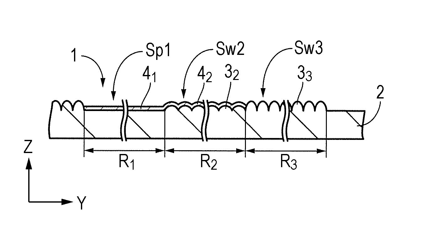
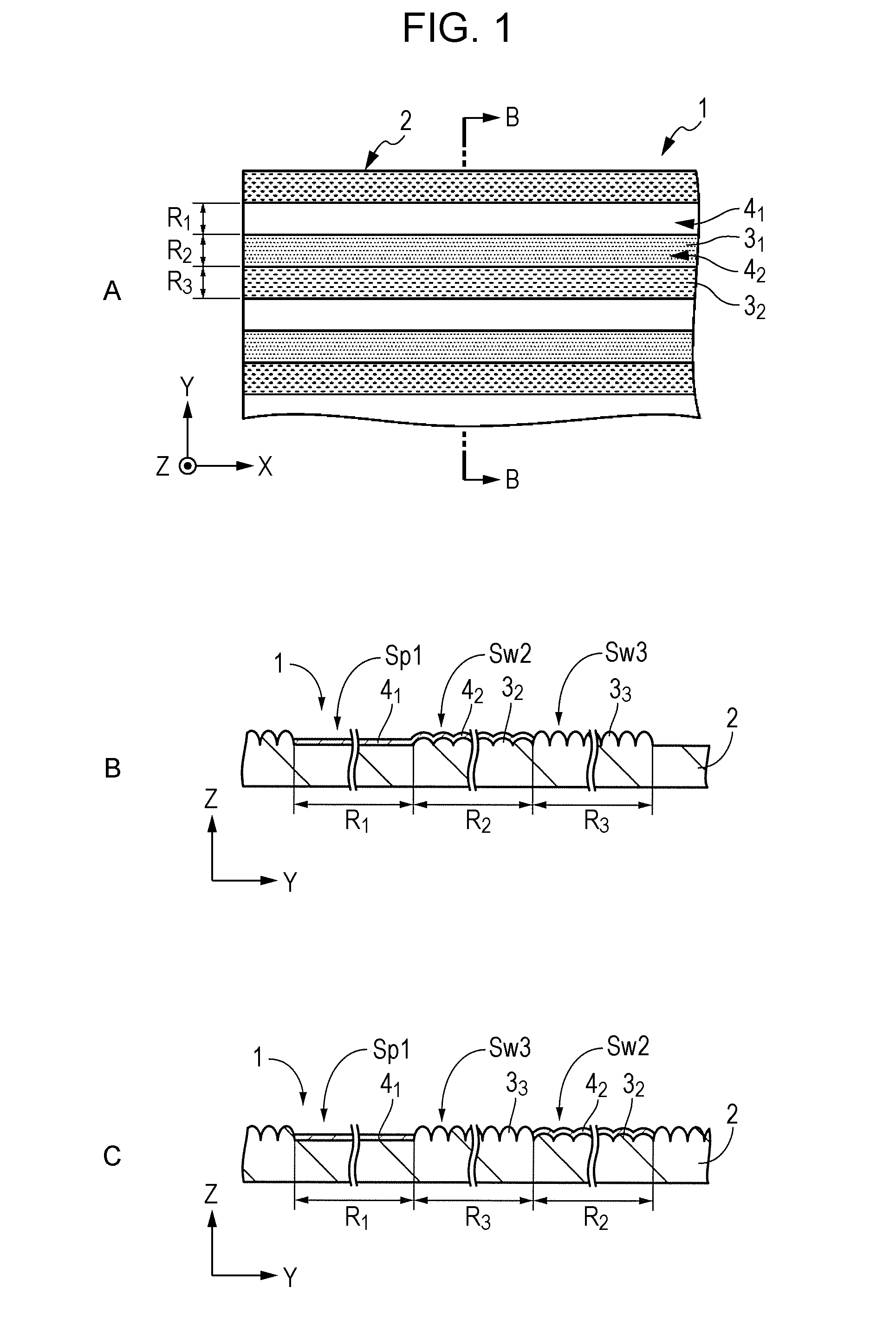
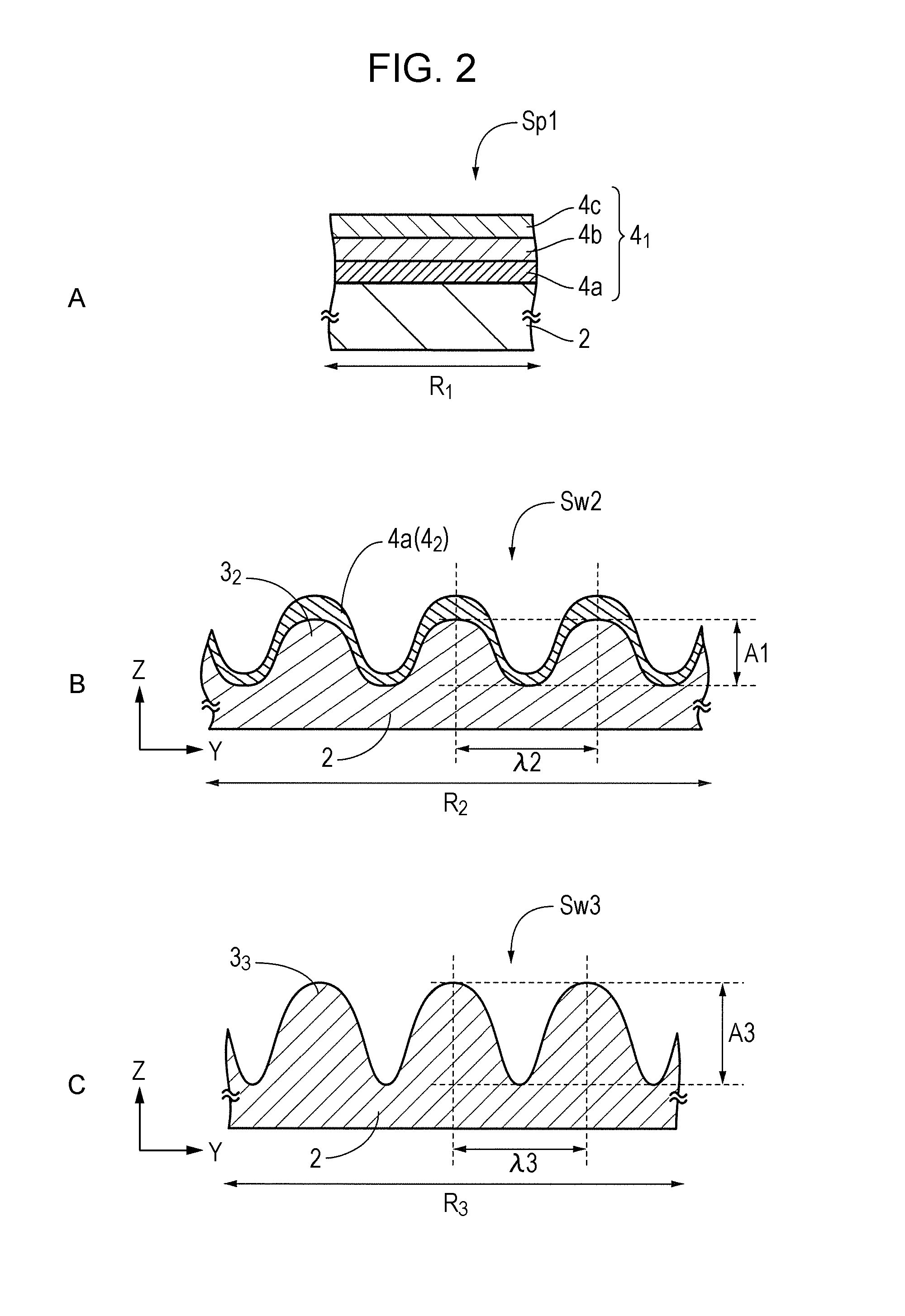
[0093]FIG. 1A is a plan view illustrating a configuration example of a conductive element according to a first embodiment of the present technology. FIG. 1B is a cross-sectional view taken along the line B-B illustrated in FIG. 1A. FIG. 2A is an enlarged cross-sectional view illustrating a part of a first region illustrated in FIG. 1B. FIG. 2B is an enlarged cross-sectional view illustrating a part of a second region illustrated in FIG. 1B. FIG. 2C is an enlarged cross-sectional view illustrating a part of a third region illustrated in FIG. 1B. Hereinafter, two directions which are orthogonal to each other on a plane of the principal surface of a conductive element 1 are respectively referred to as an X-axis direction and a Y-axis direction, and a direction perpendicular to the principal surface is referred to as a Z-axis direction.
[0094]The conductive element 1 according to the first embodiment includes a substrate 2 including a...
second embodiment
2. Second Embodiment
Configuration of Conductive Element
[0189]FIG. 11A is a plan view illustrating a configuration example of a conductive element according to a second embodiment of the present technology. FIG. 11B is a cross-sectional view taken along the line B-B illustrated in FIG. 11A. FIG. 12A is an enlarged cross-sectional view illustrating a part of a first region illustrated in FIG. 11B. FIG. 12B is an enlarged cross-sectional view illustrating a part of a second region illustrated in FIG. 11B. FIG. 12C is an enlarged cross-sectional view illustrating a part of a third region illustrated in FIG. 11B. A conductive element 1 according to the second embodiment is different from that of the first embodiment in that the first region has a wavy surface Sw1. On the surface of the substrate 2, for example, a shape layer having the wavy surface Sw1, a wavy surface Sw2, and a wavy surface Sw3 is provided. The shape layer includes a structure 31, a structure 32, and a structure 3, whic...
third embodiment
3. Third Embodiment
Configuration of Conductive Element
[0214]FIG. 14A is a plan view illustrating a configuration example of a conductive element according to a third embodiment of the present technology. FIG. 14B is a cross-sectional view taken along the line B-B illustrated in FIG. 14A. FIG. 14C is an enlarged cross-sectional view illustrating a part of a first region illustrated in FIG. 14B. FIG. 14D is an enlarged cross-sectional view illustrating a part of a second region illustrated in FIG. 14B. Hereinafter, two directions which are orthogonal to each other on a plane of the principal surface of a conductive element 1 are respectively referred to as an X-axis direction and a Y-axis direction, and a direction perpendicular to the principal surface is referred to as a Z-axis direction.
[0215]The conductive element 1 according to the third embodiment includes a substrate 2 having a first region R1 and a second region R2 which are alternately formed, and a laminated film 4 formed in...
PUM
| Property | Measurement | Unit |
|---|---|---|
| Wavelength | aaaaa | aaaaa |
| Thickness | aaaaa | aaaaa |
| Degree of polymerization | aaaaa | aaaaa |
Abstract
Description
Claims
Application Information