

Methods of forming films including germanium tin and structures and devices including the films
- Summary
- Abstract
- Description
- Claims
- Application Information
AI Technical Summary
Benefits of technology
Problems solved by technology
Method used
Image

Examples
Embodiment Construction
[0020]The description of exemplary embodiments of methods, structures, and devices provided below is merely exemplary and is intended for purposes of illustration only; the following description is not intended to limit the scope of the disclosure or the claims. Moreover, recitation of multiple embodiments having stated features is not intended to exclude other embodiments having additional features or other embodiments incorporating different combinations of the stated features.
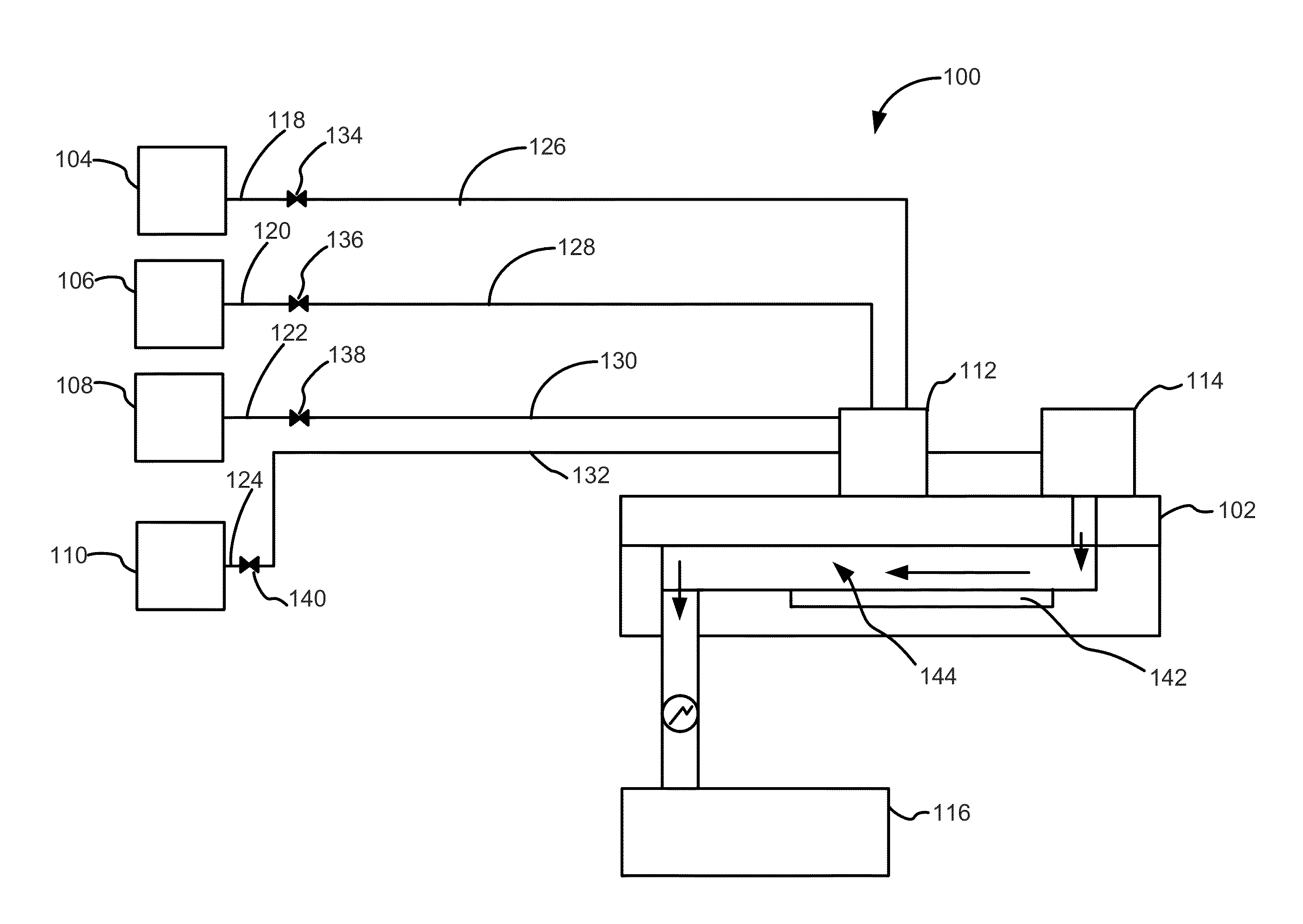
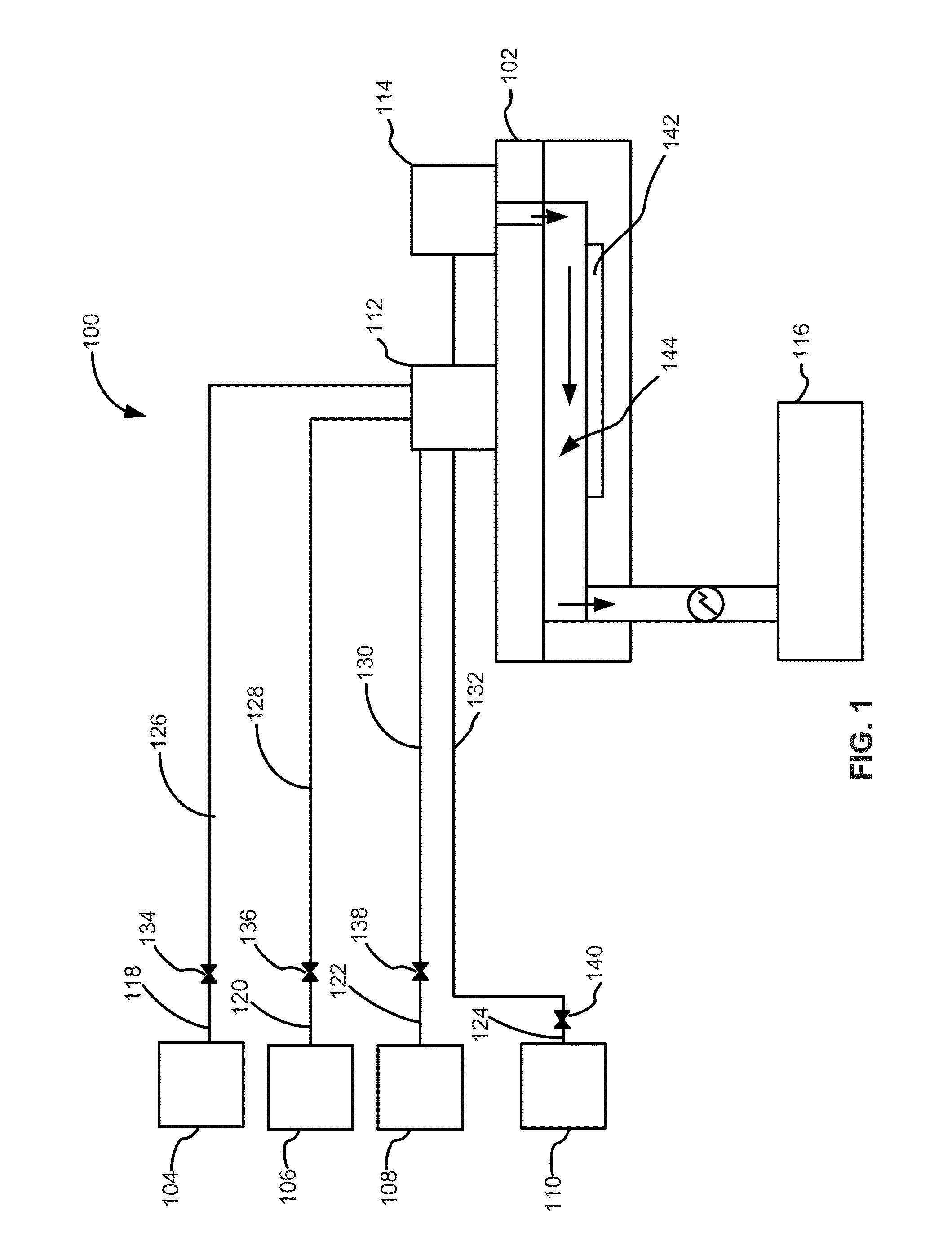
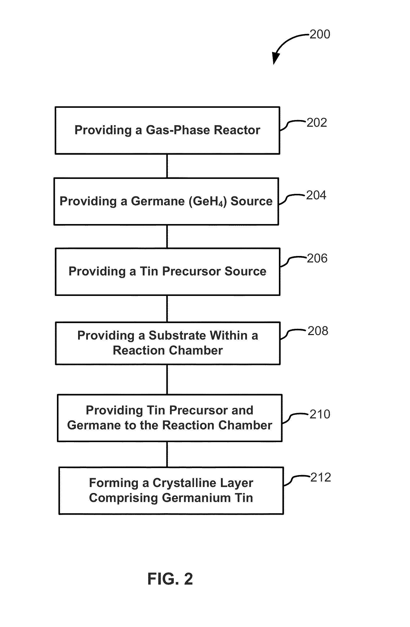
[0021]The present disclosure relates, generally, to methods of forming layers, such as a crystalline layer, including germanium and tin, overlying a substrate. The germanium-tin layers may include additional elements, such as silicon, which form part of a crystalline lattice with the germanium-tin layer.
[0022]As used herein, a “substrate” refers to any material having a surface onto which material can be deposited. A substrate may include a bulk material such as silicon (e.g., single crystal silicon, single ...
PUM
 Abstract
Description
Claims
Application Information