Production method for a semiconductor device

a production method and semiconductor technology, applied in the direction of semiconductor devices, basic electric elements, electrical appliances, etc., can solve the problems of increasing leakage current, deteriorating the characteristics of remaining defects, and generating crystal defects in silicon substrates, so as to prevent deterioration of characteristics, improve the rate of change into a donor, and avoid crystal defects. , the effect of increasing the crystal defect ra

Active Publication Date: 2015-02-19
FUJI ELECTRIC CO LTD
View PDF1 Cites 22 Cited by
  • Summary
  • Abstract
  • Description
  • Claims
  • Application Information

AI Technical Summary

Benefits of technology

[0035]According to the method for producing a semiconductor device of the invention, in the generation of donors by proton implantation, it is possible to introduce hydrogen into the silicon substrate, without increasing the crystal defects, and to prevent...

Problems solved by technology

It has been known that crystal defects are generated in the silicon substrate by the proton implantation.
The crystal defect is inevitable in the generation of donors and causes deterioration of electric characteristics which cause an increase in leakage current, depending on, for example, the kind or concentration of defects.
Therefore, the remaining defect deteriorates the characteristics of the element.
In addition, the remaining defect becomes the generation center of carriers and incr...

Method used


Image

  • Production method for a semiconductor device
  • Production method for a semiconductor device
  • Production method for a semiconductor device

Examples


first embodiment

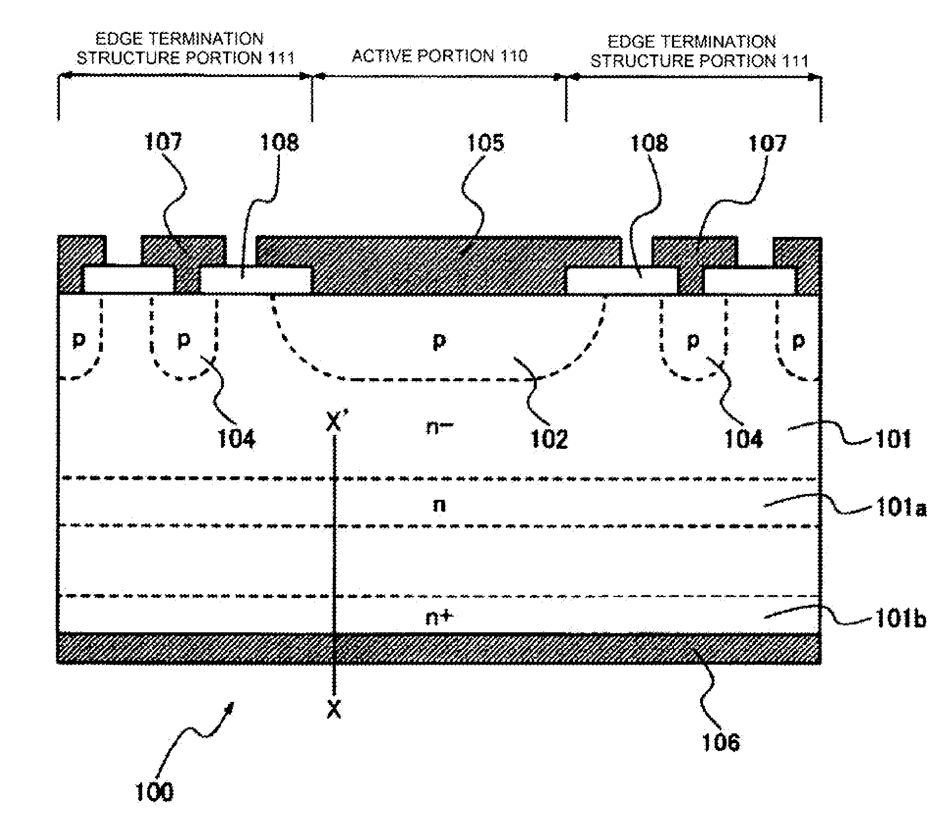
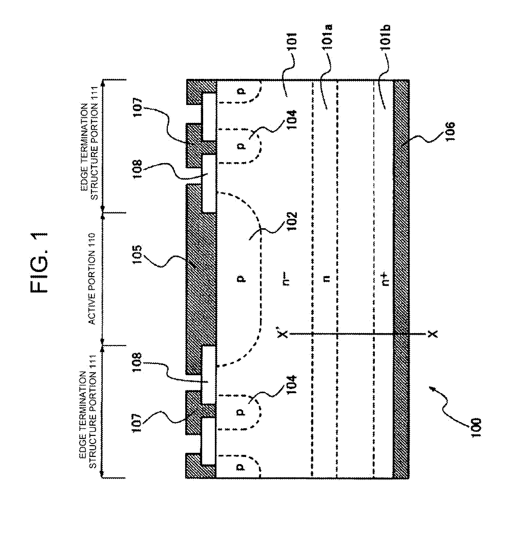
[0061]FIG. 1 is a cross-sectional view illustrating a diode as a semiconductor device according to the invention. An example of a semiconductor device 100 illustrated in FIG. 1 is a diode. However, the semiconductor device 100 may be an insulated gate bipolar transistor (IGBT).

[0062]In the semiconductor device 100, a p-type anode layer 102 is formed in a surface layer of a main surface of an n− semiconductor substrate (n− drift region) 101 and an n+ cathode layer 101b is formed in a surface layer of an opposite surface (rear surface). A p-type layer, which will be a termination region 104, is formed in the outer circumference of the p-type anode layer 102. The semiconductor device 100 controls the doping concentration of n-type impurities at a deep position from the front surface to the rear surface in order to reduce voltage oscillation which causes noise during switching.

[0063]FIG. 1 illustrates a state in which, after proton implantation, annealing is performed in a hydrogen atmo...

example

[0073]Next, the characteristics of the semiconductor device 100 having the above-mentioned structure will be described. FIG. 9 is a characteristic diagram illustrating the measurement result of a carrier concentration distribution in the depth direction after annealing in the process of producing the active portion of the diode according to the first embodiment. FIG. 9 illustrates the measurement result of the carrier concentration distribution in a portion corresponding to the X-X′ axis of FIG. 1 by a spreading resistance analysis (SRA) method when annealing is performed at a hydrogen concentration of 0% and 4% in a proton furnace (which holds for FIGS. 22 to 24). The carrier concentration measured by the SRA method substantially indicates doping concentration when the mobility of carriers is equal to an ideal value of a crystal. In contrast, when there are many crystal defects or crystal disorder is large, mobility is reduced. Therefore, spreading resistance increases and low carr...

second embodiment

[0078]Next, a method for producing a semiconductor device according to a second embodiment will be described. The method for producing the semiconductor device according to the second embodiment differs from the method for producing the semiconductor device according to the first embodiment in the acceleration energy and annealing conditions of a proton. The method for producing the semiconductor device according to the second embodiment is the same as the method for producing the semiconductor device according to the first embodiment except for proton annealing conditions.

[0079]Specifically, first, similarly to the first embodiment, a process from the formation of a p-type anode layer 102 to the implantation of a proton 601 is performed (FIGS. 2 to 6). The acceleration energy of the proton is, for example, 1.1 MeV (a range Rp is 18 μm). Then, for example, annealing 701 is performed at a temperature of 340° C. for 10 hours in an atmosphere in which hydrogen concentration is equal to...


PUM


Abstract

A method for producing a semiconductor device includes providing a semiconductor substrate having a first conductivity type; implanting protons through a rear surface of the semiconductor substrate of the first conductivity type; and forming a first semiconductor region of the first conductivity type in the semiconductor substrate by performing an annealing process in an annealing furnace in a hydrogen atmosphere having a volume concentration of hydrogen that is equal to or greater than 0.5% and less than 4.65%, the first semiconductor region having a higher impurity concentration than that of the semiconductor substrate after the implantation step. The method reduces crystal defects in the generation of donors during proton implantation and improves the rate of change into a donor.

Description

TECHNICAL FIELD[0001]The present invention relates to a method for producing a semiconductor device.BACKGROUND ART[0002]As a power semiconductor device, for example, there is a diode or an insulated gate bipolar transistor (IGBT) with a breakdown voltage of 400 V, 600 V, 1200 V, 1700 V, 3300 V, or more. The power semiconductor device is used in a power conversion device, such as a converter or an inverter. The power semiconductor device requires characteristics, such as low loss, high efficiency, a high breakdown voltage, and low costs.[0003]FIG. 12 is a cross-sectional view illustrating a diode according to the related art. A p-type anode layer 1501 is formed on a main surface of an n− semiconductor substrate 1500 and an n+ cathode layer 1502 is formed on an opposite surface. A p-type layer which will be a termination region 1503 is formed in the outer circumference of the p-type anode layer 1501. An anode electrode 1505 is formed on the p-type anode layer 1501 and a cathode electr...

Claims


Application Information

Patent Timeline
IPC IPC(8): H01L21/322
CPCH01L21/3223H01L29/32H01L29/36H01L29/66128H01L29/66348H01L29/7397H01L29/8611H01L21/263H01L21/324H01L29/402H01L29/0619
Inventor KOBAYASHI, YUSUKEYOSHIMURA, TAKASHI
Owner FUJI ELECTRIC CO LTD
Why Eureka
Try Eureka