Method to Form a Polysilicon Nanocrystal Thin Film Storage Bitcell within a High K Metal Gate Platform Technology Using a Gate Last Process to Form Transistor Gates

a technology of polysilicon nanocrystal and storage bitcell, which is applied in the field of integrated circuit devices, can solve problems such as feature sizes

Active Publication Date: 2015-02-26
NXP USA INC
View PDF20 Cites 23 Cited by
  • Summary
  • Abstract
  • Description
  • Claims
  • Application Information

AI Technical Summary

Problems solved by technology

While the introduction of novel gate stack materials for forming high-k metal gate stacks using gate last processes has improved device performance and reduced feature sizes for transistor devices, there are a number of integration options and challenges associated with the integration of such novel materials with existing polysilicon nanocrystal thin film storage bitcells.

Method used


Image

  • Method to Form a Polysilicon Nanocrystal Thin Film Storage Bitcell within a High K Metal Gate Platform Technology Using a Gate Last Process to Form Transistor Gates
  • Method to Form a Polysilicon Nanocrystal Thin Film Storage Bitcell within a High K Metal Gate Platform Technology Using a Gate Last Process to Form Transistor Gates
  • Method to Form a Polysilicon Nanocrystal Thin Film Storage Bitcell within a High K Metal Gate Platform Technology Using a Gate Last Process to Form Transistor Gates

Examples


Embodiment Construction

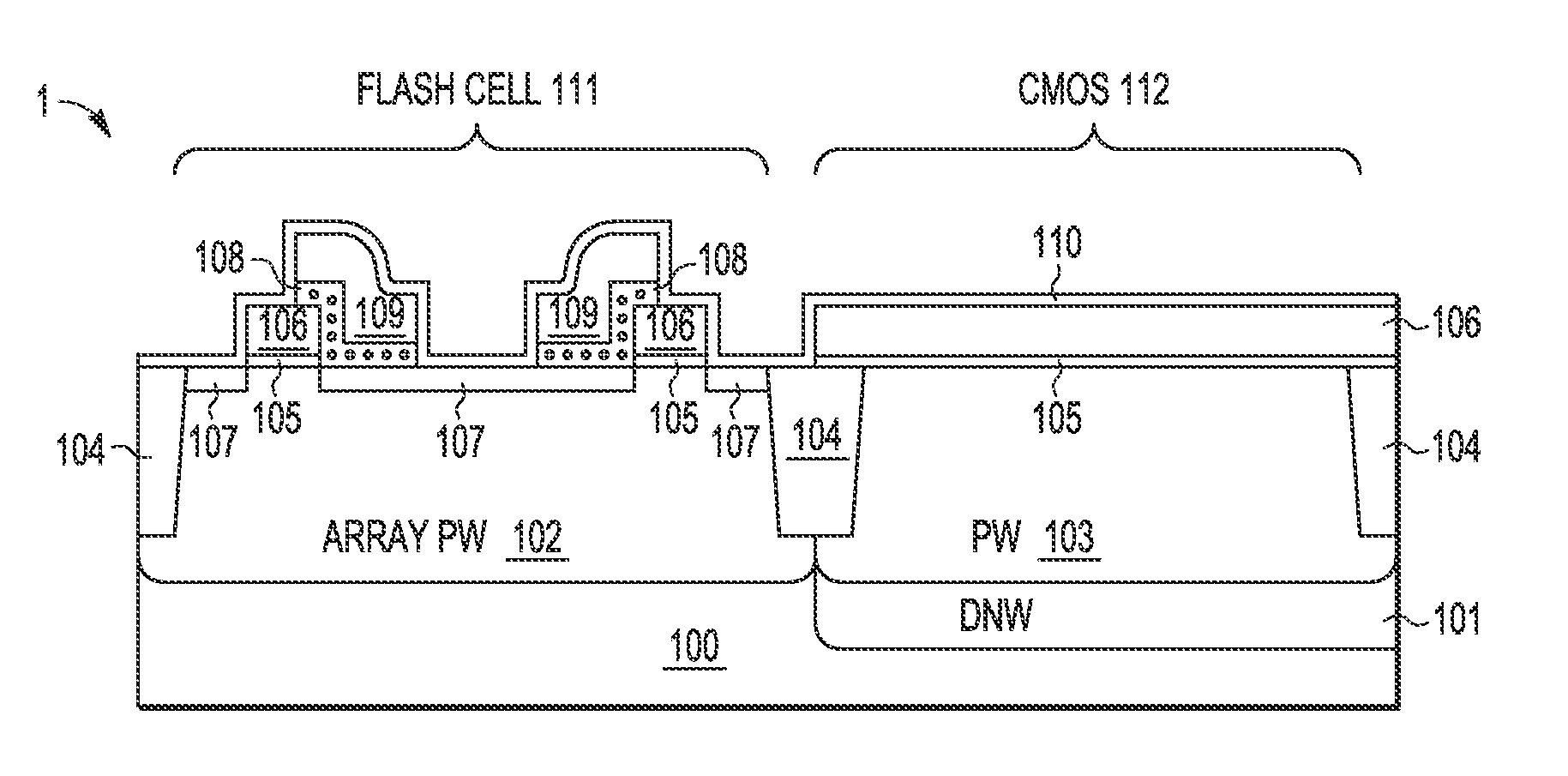
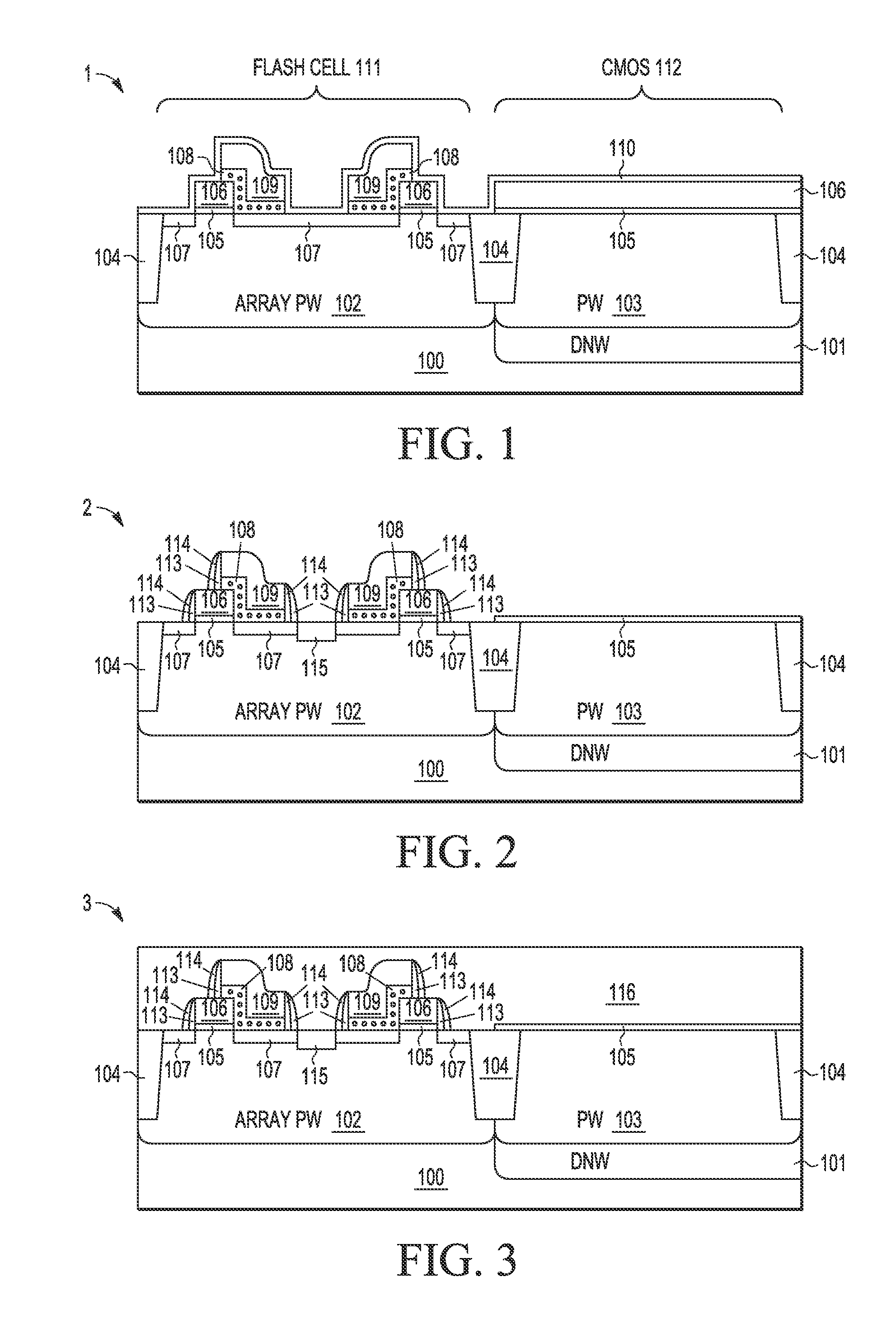
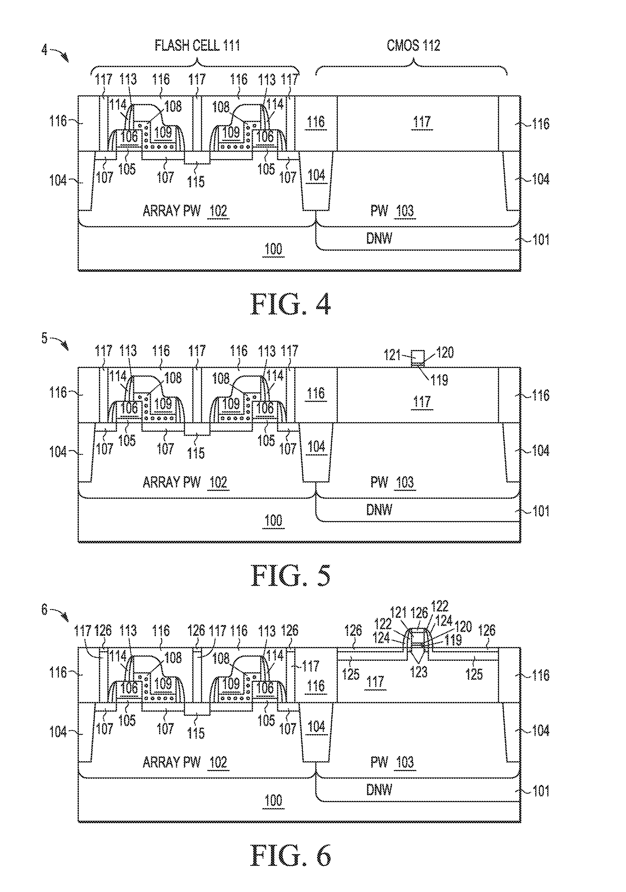
[0012]A compact split-gate polysilicon nanocrystal thin film storage (TFS) non-volatile memory (NVM) bitcell integrated with high-k metal gate (HKMG) transistors and associated fabrication process are disclosed in which selective epitaxial growth is used to elevate a wafer surface where HKMG transistors will be formed relative to the NVM bitcell to provide CMOS logic with on-chip non-volatile memory storage using a CMOS gate-last fabrication sequence, thereby enabling the co-existence of embedded flash and HKMG transistors on the same wafer. By encapsulating the NVM bitcell with a planar oxide layer prior to epitaxially growing or elevating the wafer surface in the HKMG transistor area, the NVM bitcell may be isolated from the metal gate processing and related metallic contamination used to form HKMG devices in the same gate last process flow. Selected embodiments of the disclosed integration scheme encapsulate polysilicon-nitrided-silicon dioxide (“poly-SiON”) TFS bitcells in an NV...


PUM


Abstract

A process integration is disclosed for fabricating non-volatile memory (NVM) cells (105-109, 113-115) on a first flash cell substrate area (111) which are encapsulated in one or more planar dielectric layers (116) prior to forming an elevated substrate (117) on a second CMOS transistor area (112) on which high-k metal gate electrodes (119-120, 122-126, 132, 134) are formed using a gate-last HKMG CMOS process flow without interfering with the operation or reliability of the NVM cells.

Description

BACKGROUND OF THE INVENTION[0001]1. Field of the Invention[0002]The present invention is directed in general to integrated circuit devices and methods for manufacturing same. In one aspect, the present invention relates to the fabrication of CMOS metal gate devices and non-volatile memory devices integrated on a single substrate or chip.[0003]2. Description of the Related Art[0004]Non-volatile memory devices, such as EEPROM and flash memory, are used in computers and other electronic devices to store data and / or programming instructions that can be electrically erased and reprogrammed and that must be saved when power is removed. Embedded non-volatile memory (NVM) has become increasingly important in applications ranging from data and code storage to circuit trimming and customization. By embedding a non-volatile memory in a CMOS device, a single chip device can be manufactured and configured for a variety of applications. While the introduction of novel gate stack materials for for...

Claims


Application Information

Patent Timeline
Patent Type & Authority Applications(United States)
IPC IPC(8): H01L27/115H01L21/28
CPCH01L21/28273H01L27/11578H01L29/42332H01L29/66825H01L29/7881H01L29/66545H01L29/40114H10B41/43
Inventor PERERA, ASANGA H.KANG, SUNG-TAEGYATER, JANE A.HONG, CHEONG MIN
Owner NXP USA INC
Why Eureka
Try Eureka