Low noise capacitive sensor with integrated bandpass filter

a capacitive sensor and filter technology, applied in the field of low noise, current mode capacitive sensor having an integrated bandpass filter, can solve the problems of significant array noise, significant circuit performance change, and several significant circuit limitations of fig. 1b

Active Publication Date: 2015-02-26
TEXAS INSTR INC
View PDF4 Cites 9 Cited by
  • Summary
  • Abstract
  • Description
  • Claims
  • Application Information

AI Technical Summary

Benefits of technology

[0019]The preferred embodiments of the present invention provide significant advantages over touch screen circuits of the prior art as will become evident from the following detailed description.

Problems solved by technology

There are several problems, however, with this touch screen system.
First, row and column selection in the touch screen array produces significant array noise that is coupled to sense amplifier 108.
There are several significant limitations of the circuit of FIG. 1B.
Thus, minor process variations may significantly alter circuit performance.
Although amplifier GAIN increases with K, it can not be very high or the circuit becomes unstable.
Moreover, when K is greater than 1, the circuit does not operate with unity feedback, and total harmonic distortion (THD) increases.

Method used


Image

  • Low noise capacitive sensor with integrated bandpass filter
  • Low noise capacitive sensor with integrated bandpass filter
  • Low noise capacitive sensor with integrated bandpass filter

Examples


second embodiment

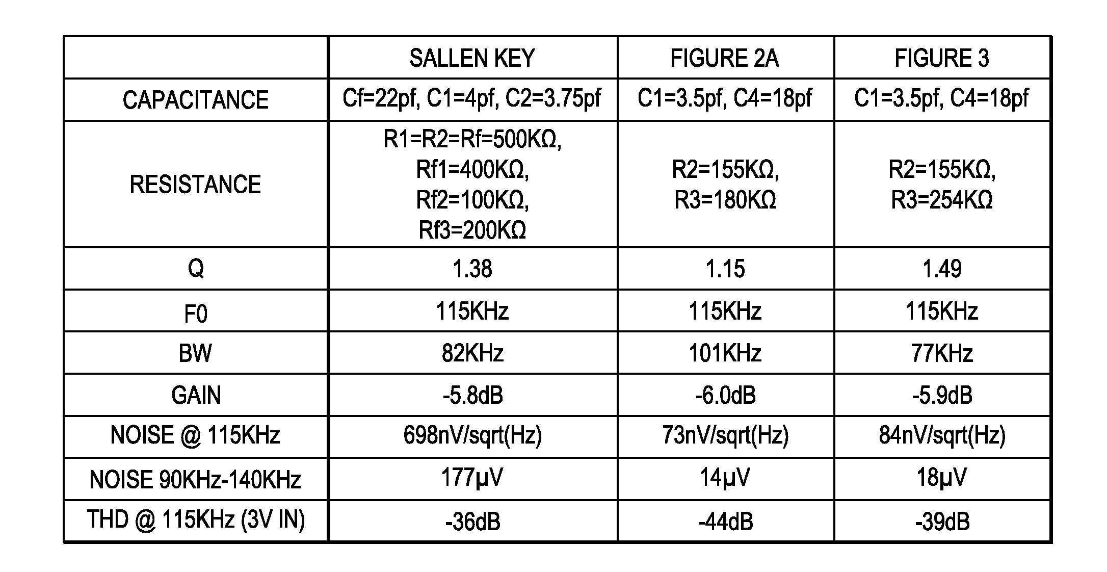
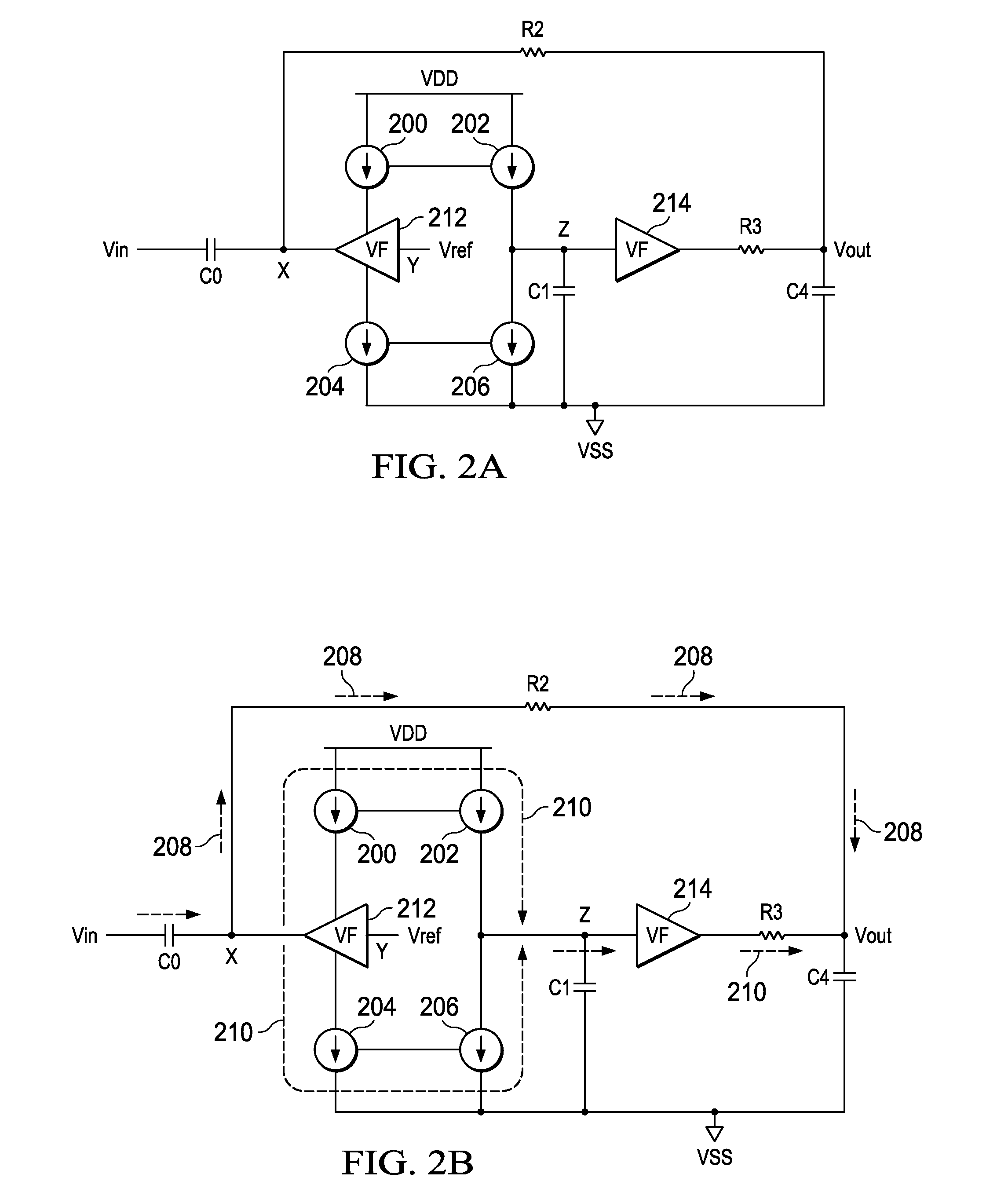
[0026]Turning now to FIG. 3, there is a circuit diagram of a bandpass sense amplifier of the present invention. This embodiment is similar to the embodiment of FIG. 2A. However, a second current conveyor circuit including current sources 300 through 306 and voltage follower circuit 308 replace voltage follower 214. Here, the voltage at terminal Z is reproduced at the output terminal of voltage follower 308. The current into the output terminal of voltage follower 308 from current sources 300 and 304 is mirrored into the sense amplifier output terminal at capacitor C4 by current sources 302 and 306. This circuit generates slightly more noise than the circuit of FIG. 2A but less than circuits of the prior art. However, it offers an advantage of increasing sense amplifier gain by either decreasing resistor R3 or increasing resistor R2. A Laplace transform of the transfer function of the bandpass sense amplifier of FIG. 3 is given by equation [12].

H(s)=-sR2C0s2R2R3C1C4+sR3C1+1[12]

[0027]...

first embodiment

[0028]Referring next to FIG. 4A, there is a circuit diagram of a current conveyor circuit that may be used with the bandpass sense amplifiers of FIGS. 2A and 3. The circuit includes p-channel transistors 402 and 404 connected in a current mirror configuration. The circuit further includes n-channel transistors 406 and 408 also connected in a current mirror configuration. Transistors 402 through 408 are equivalent to current sources 200 through 206 (FIGS. 2A and 3), respectively. N-channel transistors 410 and 414 and p-channel transistors 412 and 416 are configured as source followers. Together with current sources 400 and 418, they are equivalent to voltage followers 212 and 214 (FIG. 2A) and 308 (FIG. 3).

[0029]FIG. 4B is a circuit diagram of a second embodiment of a current conveyor circuit that may be used with the bandpass sense amplifiers of FIGS. 2A and 3. The circuit includes p-channel transistors 424 and 426 connected in a current mirror configuration to mirror terminal X cur...

third embodiment

[0030]FIG. 4C is a circuit diagram of a current conveyor circuit that may be used with the bandpass sense amplifiers of FIGS. 2A and 3. The circuit includes p-channel transistors 446 through 452 connected in a cascode current mirror configuration with gates of transistors 450 and 452 receiving reference voltage Vr1. N-channel transistors 454 through 460 are also connected in a cascode current mirror configuration with gates of transistors 454 and 456 receiving reference voltage Vr2. Current source 440 and p-channel transistors 442 and 444 form a differential input stage to the n-channel cascode current mirror circuit. N-channel transistor 462 and p-channel transistor 464 are coupled to receive respective gate reference voltages Vr3 and Vr4. An output stage of the current conveyor circuit is formed by p-channel transistors 466 and 470 and by n-channel transistors 468 and 472.

[0031]In operation, gate to source voltage of p-channel transistor 466 is always the same as gate to source vo...


PUM


Abstract

A bandpass sense amplifier circuit (FIG. 2A) is disclosed. The circuit includes a capacitor (C0) having a first terminal coupled to receive an input signal (Vin) and a second terminal. A current conveyor circuit (200-206,212) has a third terminal (X) coupled to the second terminal of the capacitor and a fourth terminal (Z) arranged to mirror a current into the third terminal. A voltage follower circuit (214) has an input terminal coupled to the fourth terminal of the current conveyor circuit and an output terminal.

Description

BACKGROUND OF THE INVENTION[0001]Embodiments of the present invention relate to a low noise, current mode capacitive sensor having an integrated bandpass filter.[0002]Touch screen input panels are widely used in cell phones, computer tablets, laptop and desktop computers, video games, and other electronic devices. These panels may be resistive type, light sensing type, or capacitive sensing type. Referring to FIG. 1, there is a capacitive sensing touch screen input system of the prior art as disclosed by Jang et al. (U.S. Pat. No. 8,477,120). The touch screen system includes an array of touch screen cells formed over a liquid crystal display (LCD). The touch screen cells are typically formed where rows of drive electrodes are insulatively disposed proximate columns of sense electrodes. Each drive electrode includes a parasitic capacitance CDX 102. Here, X is a row number from 0 to N−1 where the array includes N rows. Likewise, each sense electrode includes a parasitic capacitance CS...

Claims


Application Information

Patent Timeline
Patent Type & Authority Applications(United States)
IPC IPC(8): G06F3/041G06F3/044H03K17/96
CPCG06F3/0418G06F3/044H03K17/962G06F3/04182G06F3/0446H03K2217/960735H03H11/11
Inventor JAIN, KARAN SINGHVENKATARAMAN, HARISH
Owner TEXAS INSTR INC
Why Eureka
Try Eureka