Photoelectric conversion device and imaging device using the same

a conversion device and photoelectric technology, applied in thermoelectric devices, solid-state devices, nano-informatics, etc., can solve the problems of slow response speed and likely residual image, and achieve the effect of not deteriorating device performance, excellent step coverage, and significant deterioration of the performance of organic photoelectric conversion materials

Active Publication Date: 2015-03-05
FUJIFILM CORP
View PDF4 Cites 7 Cited by
  • Summary
  • Abstract
  • Description
  • Claims
  • Application Information

AI Technical Summary

Benefits of technology

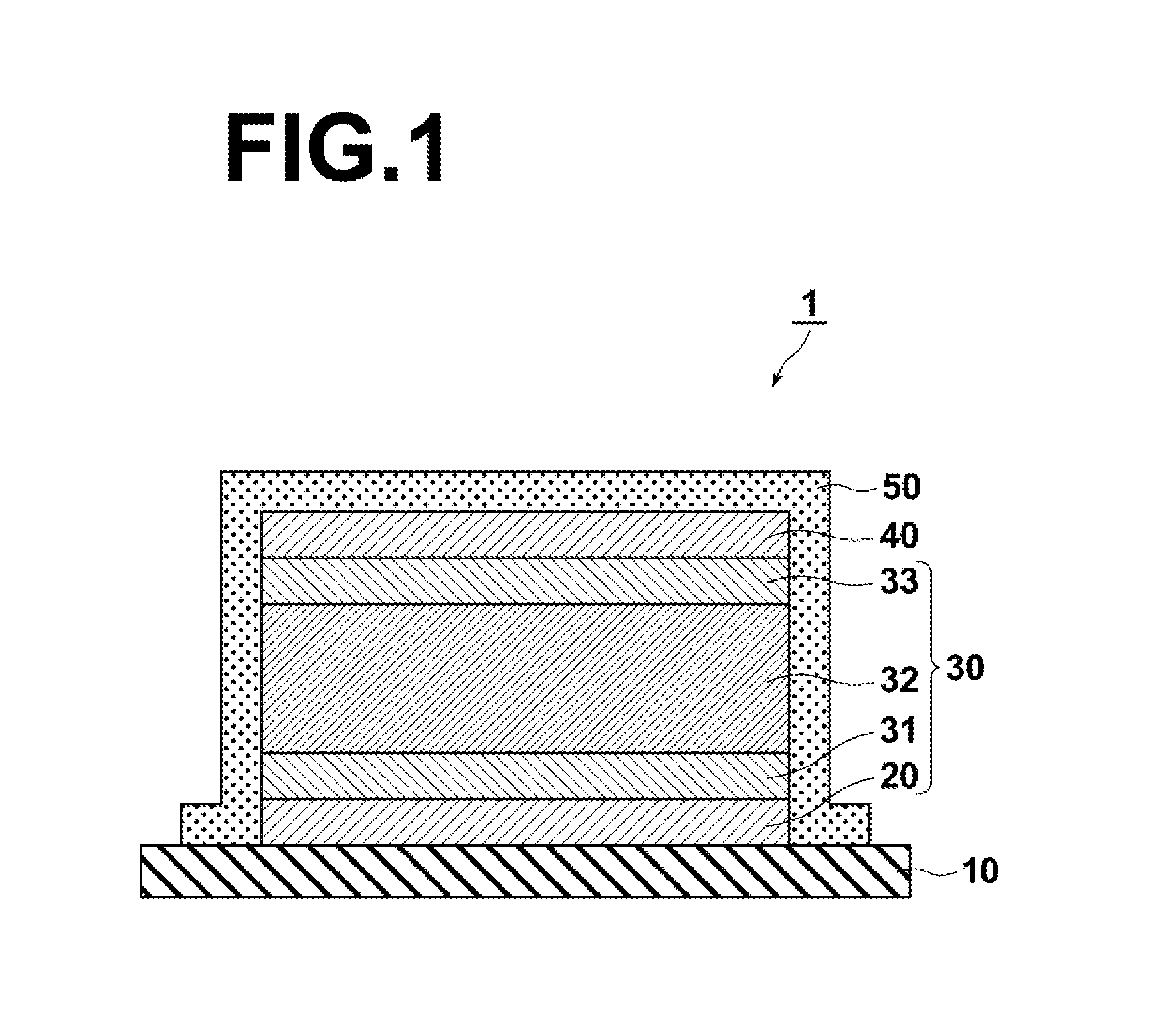
[0088]The sealing layer 50 may be formed of a thin film made of a single material, but by forming the sealing layer in a multilayer structure and giving a separate function to each layer, advantageous effects, such as stress relaxation of the entire sealing layer 50, inhibition of generation of defects, including cracks and pinholes, due to dust during the manufacturing process, ease of optimization of material development, and the like can be expected. For example, the sealing layer 50 may be formed in a two-layer structure in which a “sealing auxiliary layer” is stacked on a layer that performs the original purpose of preventing the intrusion of deterioration factors, such as water molecules, the sealing auxiliary layer being given a function which is difficult to be achieved by the layer that performs the original purpose. A three or more layer structure may be possible, but the number of layers is preferably as small as possible in view of cost.
[0089]There is not any specific restriction of the method of forming the sealing layer 50, and the sealing layer is preferably formed by a method that does not deteriorate, as much as possible, the performance and film quality of the layers already formed, such as the photoelectric conversion layer 32 and the like.
[0090]The performance of an organic photoelectric conversion material is significantly deteriorated by the presence of deterioration factors, such as water molecules and oxygen molecules. Therefore, it is necessary to cover and seal the entire photoelectric conversion layer by a dense metal oxide, a metal nitride oxide, or the like that does not allow the deterioration factors to intrude into the layer. Conventionally, aluminum oxide, silicon oxide, silicon nitride, silicon nitride oxide, a layered structure of these, and a layered structure of these and an organic polymer, and the like have been formed as sealing layers by various types of vacuum film forming techniques.
[0091]In the conventional sealing layers, however, a thin film growth is difficult on steps (due to shadows by the steps) formed by structures of the substrate surface, small defects of the substrate surface, particles adhered to the substrate surface, and the like, and the film thickness is significantly thin on the steps in comparison with a flat portion. Consequently, the step portions serve as the routes of the deterioration factors. In order to completely cover the steps with the sealing layer, it is necessary to make the entire sealing layer thick by performing the film forming with a thickness of 1 μm on the flat portion. The degree of vacuum during the formation of the sealing layer is preferably 1×10³ Pa or less and more preferably 5×10² Pa or less.
[0092]For an imaging device with a pixel size of less than 2 μm, in particular, about 1 μm, if the film thickness of the sealing layer 50 is large, the distance between the color filter and the photoelectric conversion layer is increased and incident light may diffract / diffuse within the sealing layer and color mixing may possibly occur. Therefore, in view of the application to an imaging device with a pixel size of about 1 μm, a sealing material / manufacturing method is required that does not deteriorate the device performance even when the film thickness of the sealing layer 50 is reduced.
[0093]An atomic layer deposition (ALD) method is one of the CVD methods and a technique of forming a thin film by alternately repeating adsorption / reaction of organometallic compound molecules, metal halide molecules, metal hydride molecules to the substrate surface and dissolution of unreacted groups contained therein. When reaching the substrate surface, the thin film material is in a low molecular state as described above, so that a thin film growth is possible only if there is a very small space into which the small molecules may intrude. Therefore, the atomic layer deposition method may completely cover a step portion (the thickness of the thin film grown on the step portion is the same as that grown on a flat portion) which has been difficult by conventional thin film forming methods, that is, it is very excellent in step coverage. Thus, the method can completely cover the steps formed by structures of the substrate surface, small defects of the substrate surface, particles adhered to the substrate surface, and the like, so that such steps do not serve as intrusion routes of the deterioration factors of the photoelectric conversion material. In a case where the sealing layer 50 is formed by the atomic layer deposition method, the required film thickness may be reduced more effectively than the conventional technology.

Problems solved by technology

According to the structures of Japanese Unexamined Patent Publication No. 2009-182095 and Japanese Unexamined Patent Publication No. 2012-019235, a dark current suppressing effect may be obtained, but they have a problem that the response speed is slow and a residual image is likely to occur.

Method used


Image

  • Photoelectric conversion device and imaging device using the same
  • Photoelectric conversion device and imaging device using the same
  • Photoelectric conversion device and imaging device using the same

Examples


example 2

[0117]A photoelectric conversion device was produced in the same manner as in Example 1 other than the condition of the composition of the hole blocking layer, in which the mixing ratio of Compound 1 and C60 was changed to, Compound 1:C60=1:3 (volume ratio).

example 3

[0118]A photoelectric conversion device was produced in the same manner as in Example 1 other than the condition of the composition of the hole blocking layer, in which the mixing ratio of Compound 1 and C60 was changed to, Compound 1:C60=1:1 (volume ratio).

example 4

[0119]A photoelectric conversion device was produced in the same manner as in Example 1 other than that the thickness of the hole blocking layer was changed to 20 nm.


PUM


Abstract

An organic photoelectric conversion device having a pair of electrodes and a light receiving layer which includes at least a photoelectric conversion layer and is sandwiched by the electrodes, the device including an electron blocking layer provided between the photoelectric conversion layer and one of the electrodes, and a hole blocking layer provided between the photoelectric conversion layer and the other of the electrodes, in which the hole blocking layer is a layer that includes a fullerene and / or a fullerene derivative and a transparent hole transport material having an ionization potential of 5.5 eV or more.

Description

CROSS-REFERENCE TO RELATED APPLICATIONS[0001]This application is a Continuation of PCT International Application No. PCT / JP2013 / 002914 filed on May 2, 2013, which claims priority under 35 U.S.C. §119(a) to Japanese Patent Application No. 2012-108495 filed on May 10, 2012. Each of the above applications is hereby expressly incorporated by reference, in its entirety, into the present application.BACKGROUND OF THE INVENTION[0002]1. Technical Field[0003]The present invention relates to an organic photoelectric conversion device having a photoelectric conversion layer formed of an organic layer and an imaging device equipped therewith.[0004]2. Background Art[0005]Imaging devices such as CCD sensors, CMOS sensors, and the like are known widely as image sensors used in digital still cameras, digital video cameras, cell phone cameras, endoscope cameras, and the like. These devices are equipped with a photoelectric conversion device having a light receiving layer which includes a photoelectr...

Claims


Application Information

Patent Timeline
Patent Type & Authority Applications(United States)
IPC IPC(8): H01L27/30H01L51/42H01L51/44H01L51/00
CPCH01L27/307H01L51/442H01L51/4273H01L51/0046Y02E10/549B82Y10/00H10K39/32H10K71/164H10K85/211H10K85/626H10K30/211H10K30/353H10K85/6572H10K2102/103H10K30/82
Inventor SUZUKI, HIDEYUKI
Owner FUJIFILM CORP
Why Eureka
Try Eureka