Method of Forming Different Voltage Devices with High-K Metal Gate

a technology of metal gate and high-k metal gate, which is applied in the direction of semiconductor devices, electrical equipment, transistors, etc., can solve the problems of increasing the number of integration difficulties and challenges, forming shallow trench isolation (sti) divots, and increasing the difficulty of integration

Active Publication Date: 2015-03-12
VLSI TECH LLC
View PDF1 Cites 74 Cited by
  • Summary
  • Abstract
  • Description
  • Claims
  • Application Information

AI Technical Summary

Problems solved by technology

However, the integration of non-volatile memory with CMOS transistors on a single chip can create a number of integration difficulties and challenges as the different materials and/or fabrication processes conflict with one another when the semiconductor fabrication processes used to form high voltage (HV) transistors (which handle high voltages (e.g., 12V or higher) that are suitable for programming non-volatile memory cells) or dual-gate oxide (DGO) devices (which are higher voltage, low-leakage devices suitable for battery-powered devices) are not compatible with the processes used to fabricate low voltage (LV) transistors (which are used for low-voltage logic circuits, such as microcontrollers, SRAMs, ROMs).
These challenges and difficulties can be exacerbated as device scaling increases and new device structures, such as metal gate ele

Method used


Image

  • Method of Forming Different Voltage Devices with High-K Metal Gate
  • Method of Forming Different Voltage Devices with High-K Metal Gate
  • Method of Forming Different Voltage Devices with High-K Metal Gate

Examples


Embodiment Construction

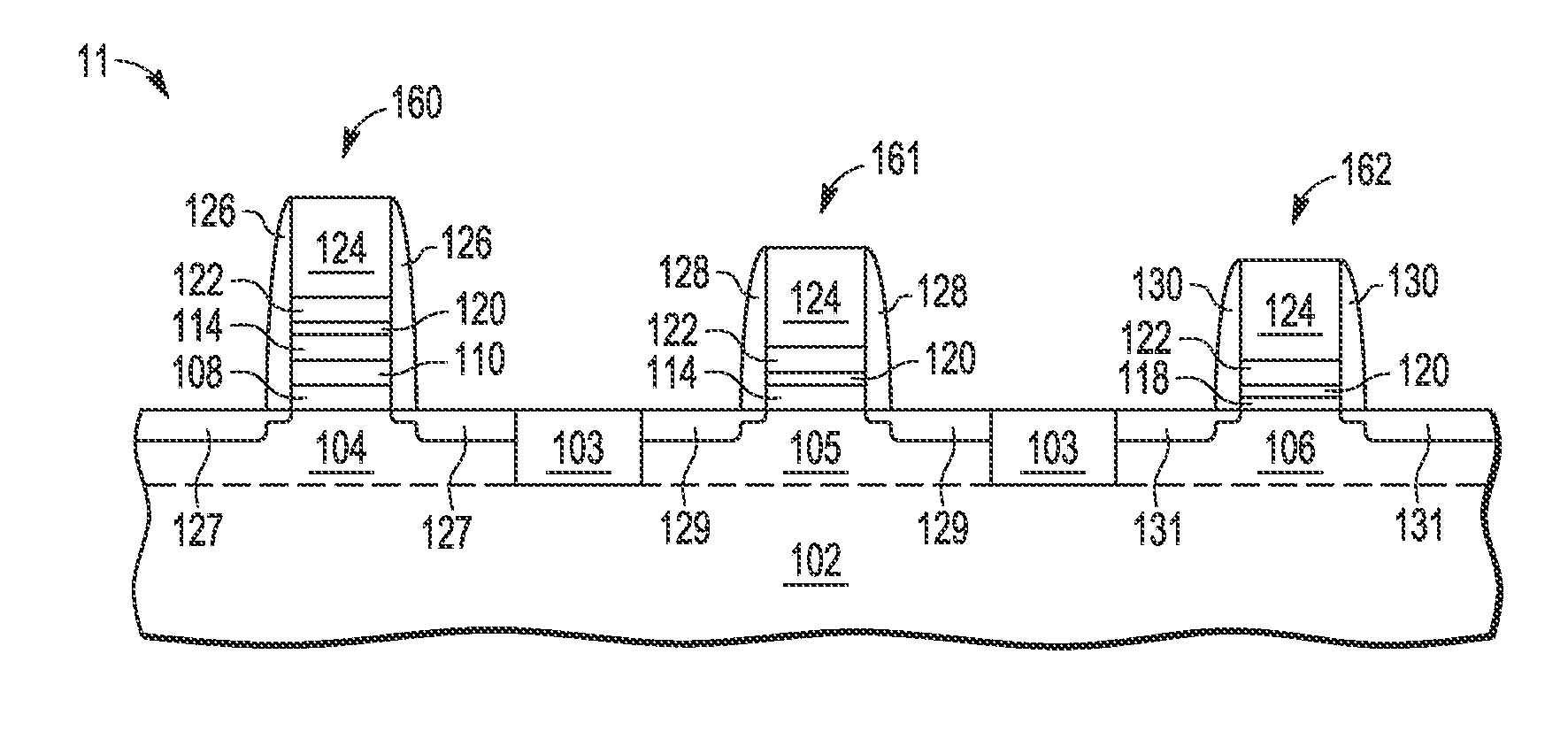
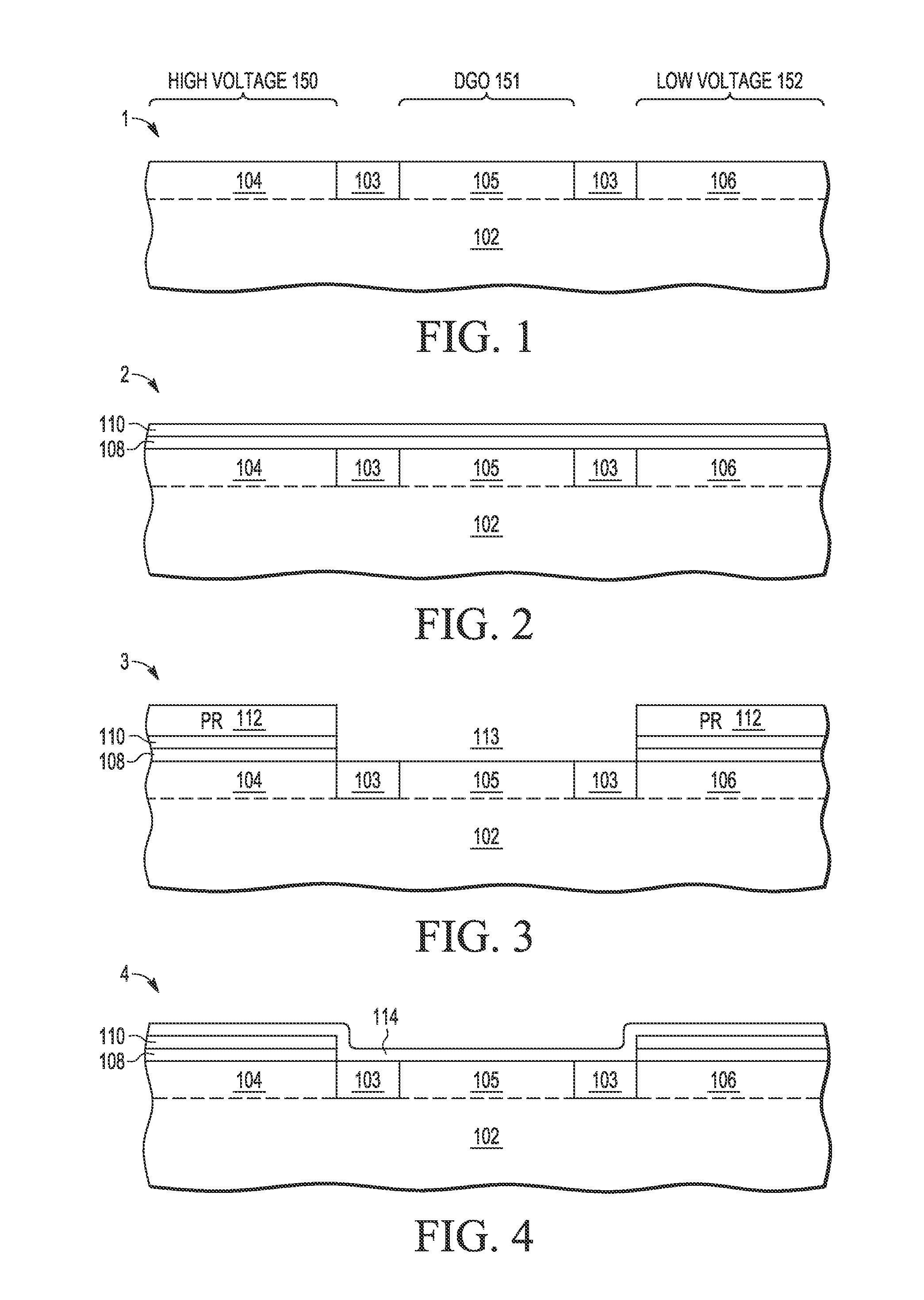
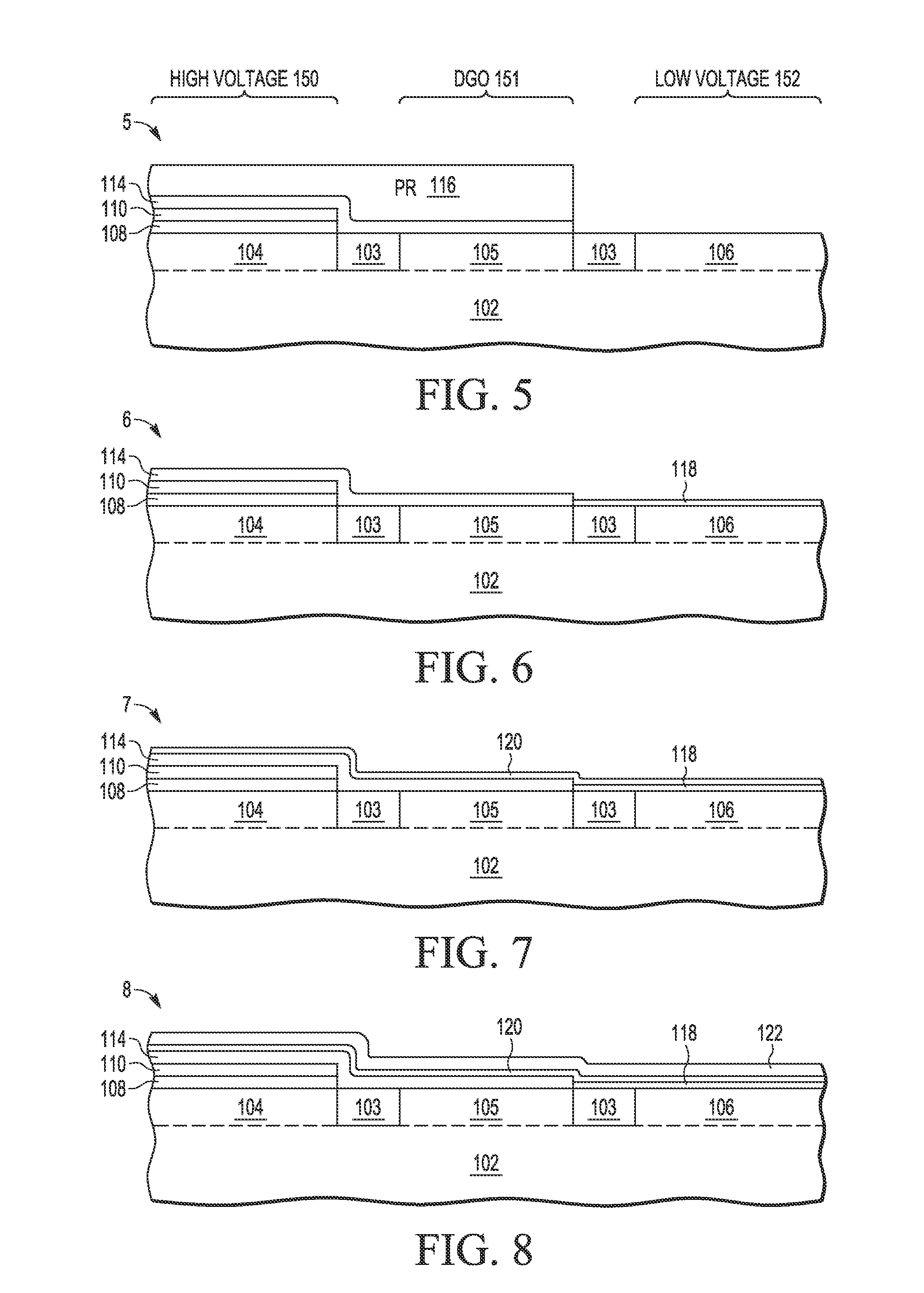
[0009]A method and apparatus are described for integrating high voltage (HV) transistor devices and medium voltage dual gate oxide (DGO) transistor devices with low voltage (LV) core transistor devices on a single substrate where each transistor includes a metal gate and one or more high-k gate dielectric layers that meet performance and reliability requirements of medium and high voltage operations while minimizing the impacts on low voltage devices. As disclosed, a high voltage gate dielectric layer is selectively formed in the high voltage and low voltage device areas of the wafer substrate to include a first thermally grown dielectric layer (e.g., thermal oxide) and a second deposited dielectric layer (e.g., deposited oxide) which are formed to a predetermined thickness to cover the high voltage and low voltage device areas, but not the medium voltage device area of the wafer substrate. With the medium voltage device area of the wafer substrate exposed, an additional dielectric ...


PUM


Abstract

A method and apparatus are described for integrating high voltage (HV) transistor devices and medium voltage or dual gate oxide (DGO) transistor devices with low voltage (LV) core transistor devices on a single substrate, where each high voltage transistor device (160) includes a metal gate (124), an upper high-k gate dielectric layer (120), a middle gate dielectric layer (114) formed with a relatively lower high-k dual gate oxide layer, and a lower high voltage gate dielectric stack (108, 110) formed with one or more low-k gate oxide layers (22), where each DGO transistor device (161) includes a metal gate (124), an upper high-k gate dielectric layer (120), and a middle gate dielectric layer (114) formed with a relatively lower high-k dual gate oxide layer, and where each core transistor device (162) includes a metal gate (124), an upper high-k gate dielectric layer (120), and a base oxide layer (118) formed with one or more low-k gate oxide layers.

Description

BACKGROUND OF THE INVENTION[0001]1. Field of the Invention[0002]The present invention is directed in general to the field of semiconductor devices and methods for manufacturing same. In one aspect, the present invention relates to the fabrication of high-k metal gate devices for different voltage level transistors integrated on a single substrate or chip.[0003]2. Description of the Related Art[0004]Non-volatile memory devices, such as EEPROM and flash memory, are used in computers and other electronic devices to store data and / or programming instructions that can be electrically erased and reprogrammed and that must be saved when power is removed. Embedded non-volatile memory (NVM) has become increasingly important in applications ranging from data and code storage to circuit trimming and customization. However, the integration of non-volatile memory with CMOS transistors on a single chip can create a number of integration difficulties and challenges as the different materials and / o...

Claims


Application Information

Patent Timeline
IPC IPC(8): H01L29/51H01L21/84H01L21/28H01L27/12
CPCH01L29/511H01L27/1203H01L21/84H01L21/28158H01L21/28194H01L29/513H01L29/517H01L29/6659H01L29/1054H01L29/165H01L21/823842H01L21/82385H01L21/823857H01L27/0922H01L29/161H01L29/518H01L29/7848
Inventor HONG, CHEONG MINPERERA, ASANGA H.KANG, SUNG-TAEG
Owner VLSI TECH LLC
Why Eureka
Try Eureka