
Metal oxide etching solution and an etching method

Inactive Publication Date: 2015-03-19
KANTO CHEM CO INC
View PDF9 Cites 13 Cited by
  • Summary
  • Abstract
  • Description
  • Claims
  • Application Information

AI Technical Summary

Benefits of technology

The present invention provides an etching solution composition that can control the etching rate for metal oxides containing In and Zn, which are commonly used in electronic devices such as displays. The composition is suitable for the formation of fine patterns and has a practical use in the production of high definition displays. Additionally, it has high dissolving power towards In and Zn, suppresses the precipitation of In and Zn in the etching solution, increases the solution life, and reduces the manufacturing cost for semiconductor elements and displays.

Problems solved by technology

However, since dry etching requires expensive vacuum equipment and a high frequency generator, it is disadvantageous in terms of cost and, in addition, there is a possibility that ions in a plasma state will damage the substrate, etc.
Furthermore, since the processed pattern cross-section has a shape in which the cross-section is vertical to or nearly vertical to the substrate, it is assumed that, when the pattern is subsequently covered using an insulating film of SiO2, etc. as an upper layer, a gap might occur between the pattern and the insulating film, or the ease of covering might be degraded.
Because of this, the processed pattern shape is often required to maintain the CD as much as possible but to have a tapered shape to some extent, and it is difficult to carry out such control by dry etching.
However, the lift-off method has the problem that a photoresist melts at high temperature and deforms.
There is another problem that, when removing the photoresist, the end of the oxide semiconductor pattern curls up, and wiring crossing over pattern ends is then easily disconnected, thus making the yield low.
Furthermore, there is the problem that pieces of resist remain after the lift-off to thus contaminate the substrate.

Method used


Image

  • Metal oxide etching solution and an etching method
  • Metal oxide etching solution and an etching method

Examples


examples

[0090]With regard to the etching solution composition of the present invention, the present invention is now explained in detail by reference to Examples and Comparative Examples, but the present invention should not be construed as being limited to these Examples, etc.

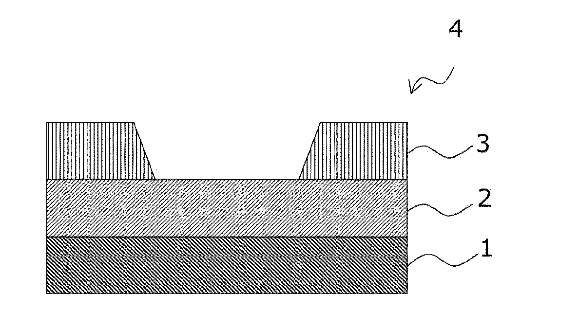
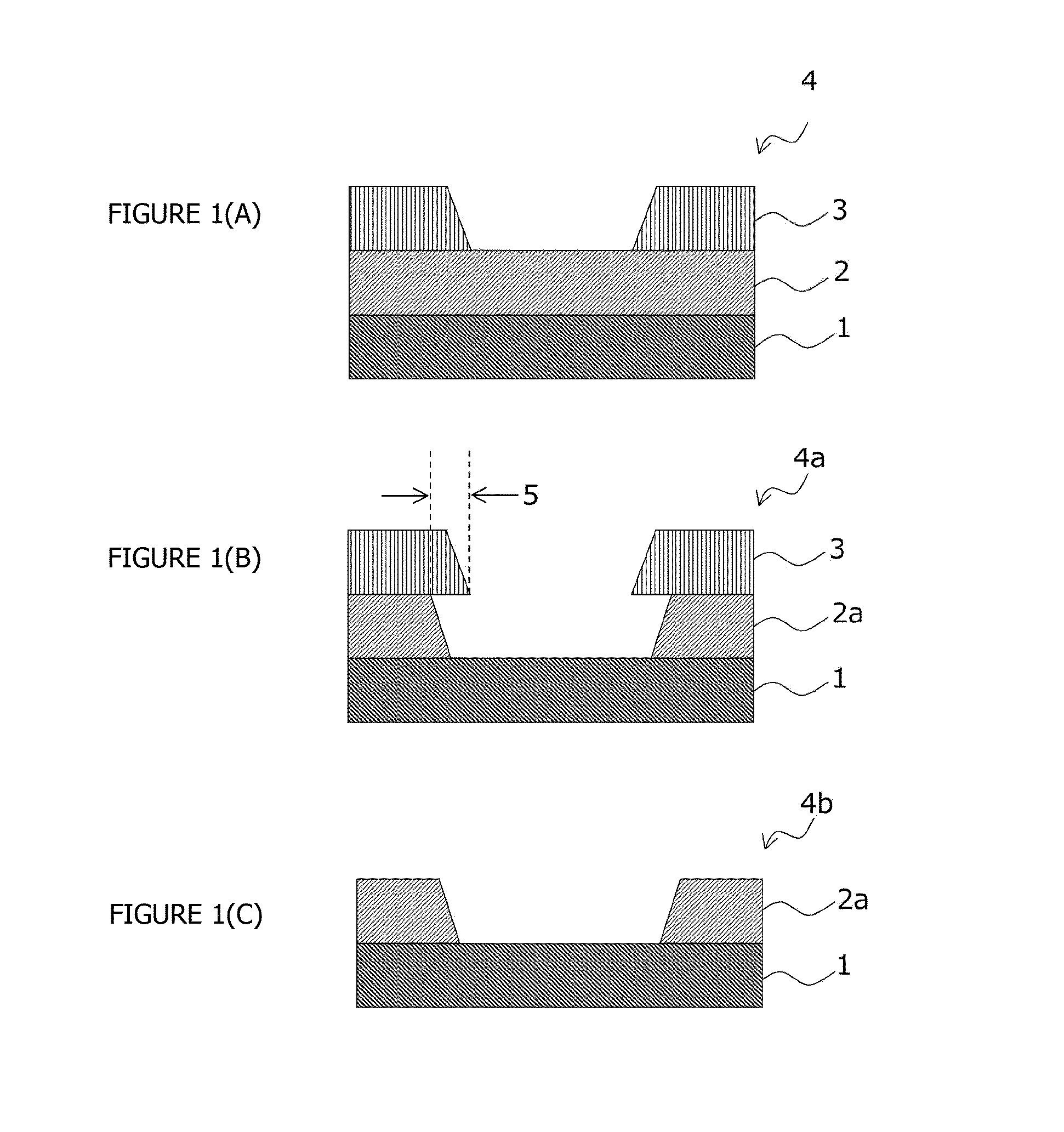
[0091]As shown in FIG. 1 (A), a 70 nm film of IZO and a 50 nm film of IGZO were formed on the surface of glass substrates 1 by a sputtering method, the surface of the sputtered film 2 was subjected to resist patterning, thus preparing two types of evaluation substrates 4, and etching solution compositions containing acids at the concentrations shown in Table 1 were prepared.

[0092]The evaluation substrate 4 was sectioned into 2.0 cm×2.0 cm pieces and immersed, while agitating, in a polyethylene container containing 50 mL of the etching solution composition at 35° C. for 10 to 60 seconds, and subjected to rinsing with ultrapure water for 1 minute and drying by blowing with nitrogen, thus giving an evaluation substrate 4...


PUM


Abstract

The object of the present invention is to provide an etching solution composition for etching a metal oxide containing In and a metal oxide containing Zn and In used as a transparent electrode or an oxide semiconductor of an electronic device such as a semiconductor element or a flat panel display (FPD), the etching solution composition being controllable to give a practical etching rate, having high dissolving power toward Zn, and enabling a long solution life due to suppressed variation of the formulation during use. The object is solved by an etching solution composition that enables microfabrication to be carried out for a metal oxide containing In and a metal oxide containing Zn and In used as a transparent electrode or an oxide semiconductor of an electronic device such as a semiconductor element or an FPD, the composition containing water and at least one type of acid, excluding hydrohalic acids, perhalic acids, etc., having an acid dissociation constant pKan at 25° C. in any dissociation stage of no greater than 2.15, and the composition having a pH at 25° C. of no greater than 4, and an etching method using the etching solution composition.

Description

TECHNICAL FIELD[0001]The present invention relates to an etching solution composition for a metal oxide used as a transparent electrode or an oxide semiconductor of an electronic device such as a semiconductor element or a flat panel display (FPD), and an etching method using the etching solution composition.BACKGROUND ART[0002]In recent years, amid the progress of miniaturization, weight reduction, and reduction in power consumption of electronic equipment, in the FPD field the introduction of an oxide semiconductor as a channel material for a thin film transistor (TFT) has been examined as a replacement for amorphous silicon (a-Si), which has been widely used in liquid crystal panels (LCD) for large TVs, etc. or low temperature polysilicon (LT p-Si), which is used in small high definition LCDs, organic EL displays (OELD), etc. Furthermore, with regard to this oxide semiconductor, IGZO, which is formed from indium (In), gallium (Ga), and zinc (Zn), has been used in practice. IGZO s...

Claims


Application Information

Patent Timeline
IPC IPC(8): C09K13/06H01L21/465H05K1/09C09K13/00C09K13/04
CPCC09K13/06C09K13/00H05K2201/0326H05K1/09H01L21/465C09K13/04H05K3/067H05K2201/10106H05K2201/10128H05K2201/10136
Inventor OHWADA, TAKUOSHIMIZU, TOSHIKAZU
Owner KANTO CHEM CO INC
Learn More