
Resistance change memory device

Active Publication Date: 2015-03-26
TOKYO INST OF TECH +1
View PDF0 Cites 18 Cited by
  • Summary
  • Abstract
  • Description
  • Claims
  • Application Information

AI Technical Summary

Benefits of technology

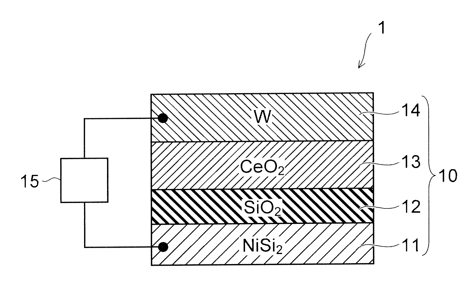
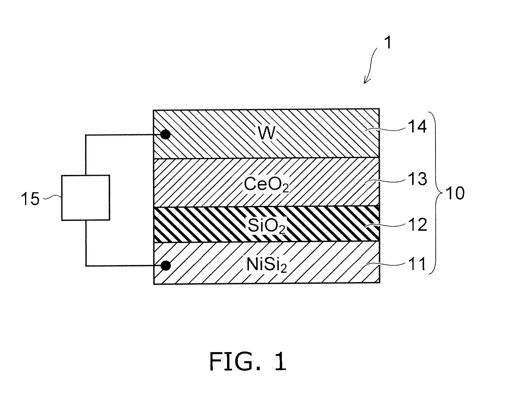
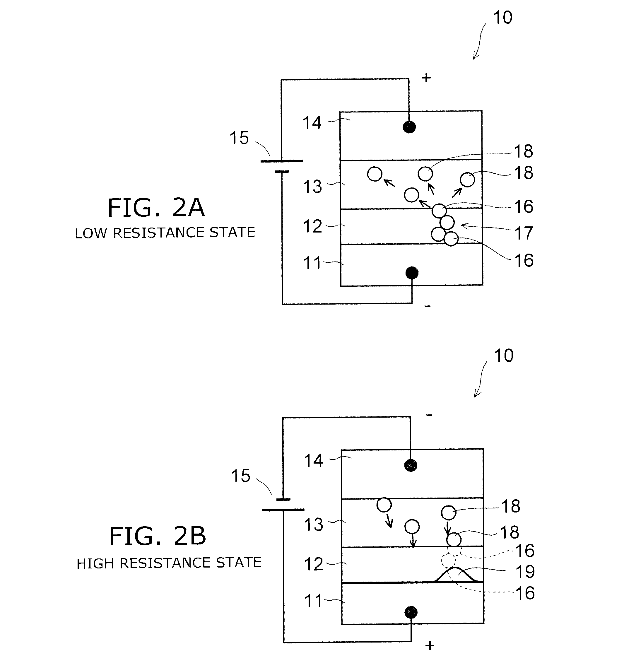
The resistance change memory device described in this patent has a unique structure that allows for fast and reliable operation. It includes a first electrode made of a first element, a resistance change layer made of an oxide of the first element, an oxygen conductive layer made of a second element and oxygen, and a second electrode made of the same material as the resistance change layer. The resistance change layer breaks down more easily than the oxygen conductive layer when a voltage is applied between the electrodes. This allows for quicker and more reliable operation of the device.

Problems solved by technology

However, such a conventional resistance change memory device has a problem that the ON / OFF ratio of the electric resistance value, that is, the value of the ratio of the magnitude of the current flowing in the lime of the low resistance state to the magnitude of the current flowing in the time of the high resistance state when a prescribed read voltage is applied, is low.
In this case, when ten memory cells are connected in series and a current is passed, even if all the memory cells are in the high resistance state, a current substantially equal to that when one memory cell is in the low resistance state flows, and it is difficult to find the value stored.
Thus, if the ON / OFF ratio is low, it is difficult to achieve higher integration of memory cells.
The forming is based on the hope that a filament will be formed in the resistance change layer incidentally; thus, the control is difficult.
However, the technologies disclosed in Non-Patent Documents 1 and 2 can only reduce the forming voltage to a level substantially equal to the set voltage or less, and cannot increase the ON / OFF ratio.
Thus, it is still difficult to achieve higher integration of memory cells.

Method used


Image

  • Resistance change memory device
  • Resistance change memory device
  • Resistance change memory device

Examples


third embodiment

[0126]FIG. 12A is a cross-sectional view showing the sample of a third example, and FIG. 12B is a graph showing the I-V characteristics of the sample, with the voltage on the horizontal axis and the current on the vertical axis.

[0127]As shown in FIG. 12A, the third example differs from the first example described above in that the oxygen conductive layer 13 is formed of a hafnium oxide (HfO2). The thickness of the hafnium oxide layer was set to 2 nm. Otherwise, the configuration of the third example is similar to the first example. That is, in the third example, the lower electrode 11 was formed of nickel disilicide (NiSi2) and the upper electrode 14 was formed of tungsten (W). A silicon oxide layer (SiO2) was formed between the nickel disilicide layer (the lower electrode 11) and the hafnium oxide layer (the oxygen conductive layer 13).

[0128]As shown in FIG. 12B, also in the third example, similar I-V characteristics to the first example were found. The ON / OFF ratio of the third ex...

fourth example

[0129]FIG. 13A is a cross-sectional view showing the sample of a fourth example, and FIG. 13B is a graph showing the I-V characteristics of the sample, with the voltage on the horizontal axis and the current on the vertical axis.

[0130]As shown in FIG. 13A, the fourth example differs from the first example described above in that the lower electrode 11 is formed of silicon with the conductivity type of the p+-type and the oxygen conductive layer 13 is formed of a hafnium oxide (HfO2). The thickness of the hafnium oxide layer was set to 2 nm. Otherwise, the configuration is similar to the first example. A silicon oxide layer (SiO2) was formed between the p+-type silicon layer (the lower electrode 11) and the hafnium oxide layer (the oxygen conductive layer 13).

[0131]As shown in FIG. 13B, also in the fourth example, similar I-V characteristics to the first example were found. The ON / OFF ratio of the fourth example was 2×10⁵ when the read potential was set to −0.1 V. Thus, a high ON / OFF...


PUM


Abstract

A resistance change memory device with a high ON / OFF ratio can be provided.A resistance change memory device according to an embodiment includes a first electrode containing a first element, a resistance change layer provided on the first electrode and containing an oxide of the first element, an oxygen conductive layer provided on the resistance change layer, containing a second element and oxygen, having oxygen ion conductivity, and having a relative permittivity higher than a relative permittivity of the resistance change layer, and a second electrode provided on the oxygen conductive layer. The resistance change layer undergoes dielectric breakdown earlier than the oxygen conductive layer when a voltage between the first electrode and the second electrode is continuously increased from zero.

Description

TECHNICAL FIELD[0001]This invention relates to a resistance change device.BACKGROUND ART[0002]These days, a phenomenon in which, when a voltage is applied to some kinds of metal oxide, the electric resistance value of the metal oxide changes between values at two levels has been found, and a memory device utilizing this phenomenon is proposed. Such a memory device is called a resistance change memory device (resistance random access memory; ReRAM).[0003]FIGS. 14A to 14C are diagrams schematically showing operations of a conventional resistance change memory device. FIG. 14A shows an initial state, FIG. 14B shows a low resistance state, and FIG. 14C shows a high resistance state.[0004]FIG. 15 is a graph illustrating the I-V characteristics of the conventional resistance change memory device, with the voltage on the horizontal axis and the current on the vertical axis.[0005]As shown in FIG. 14A, in a memory cell 110 of a conventional resistance change memory device 101, a lower electr...

Claims


Application Information

Patent Timeline
IPC IPC(8): H01L45/00
CPCH01L45/08H01L45/1233H01L45/1253H01L45/146H10N70/24H10N70/801H10N70/826H10N70/841H10N70/883H10N70/028H01L27/105H10N70/8833
Inventor KAKUSHIMA, KUNIYUKIDOU, CHUNMENGAHMET, PARHATIWAI, HIROSHIKATAOKA, YOSHINORI
Owner TOKYO INST OF TECH
Learn More