
Enhanced optical modulation using slow light

a technology of enhanced optical modulation and slow light, applied in the direction of optical waveguide light guide, optical element, instrument, etc., can solve the problems of large electrical power consumption, significantly increase the cost of ring-resonator modulator, and the speed of the modulator is typically limited to around 1 gb/s

Active Publication Date: 2015-03-26
ORACLE INT CORP
View PDF1 Cites 13 Cited by
  • Summary
  • Abstract
  • Description
  • Claims
  • Application Information

AI Technical Summary

Benefits of technology

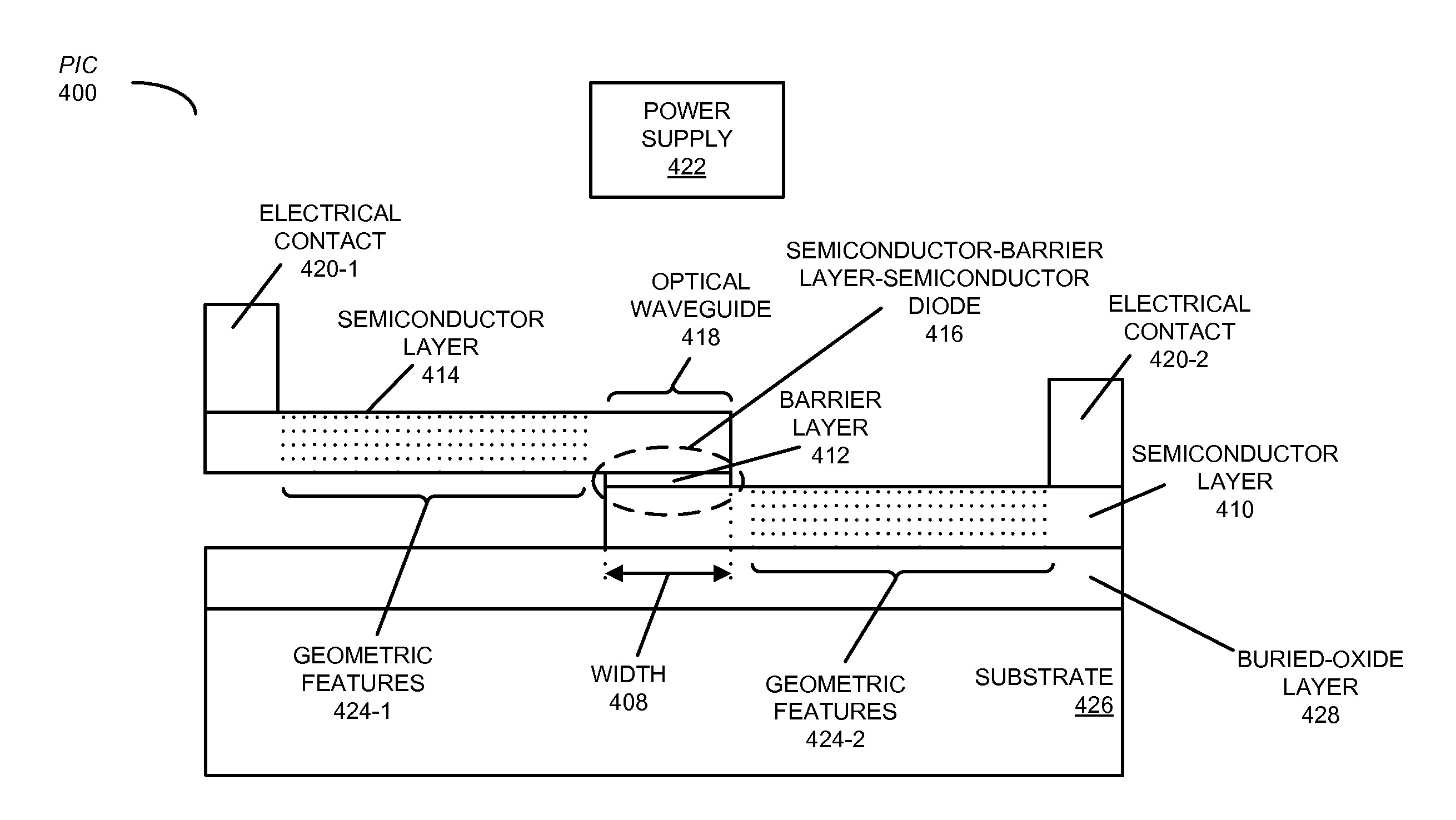
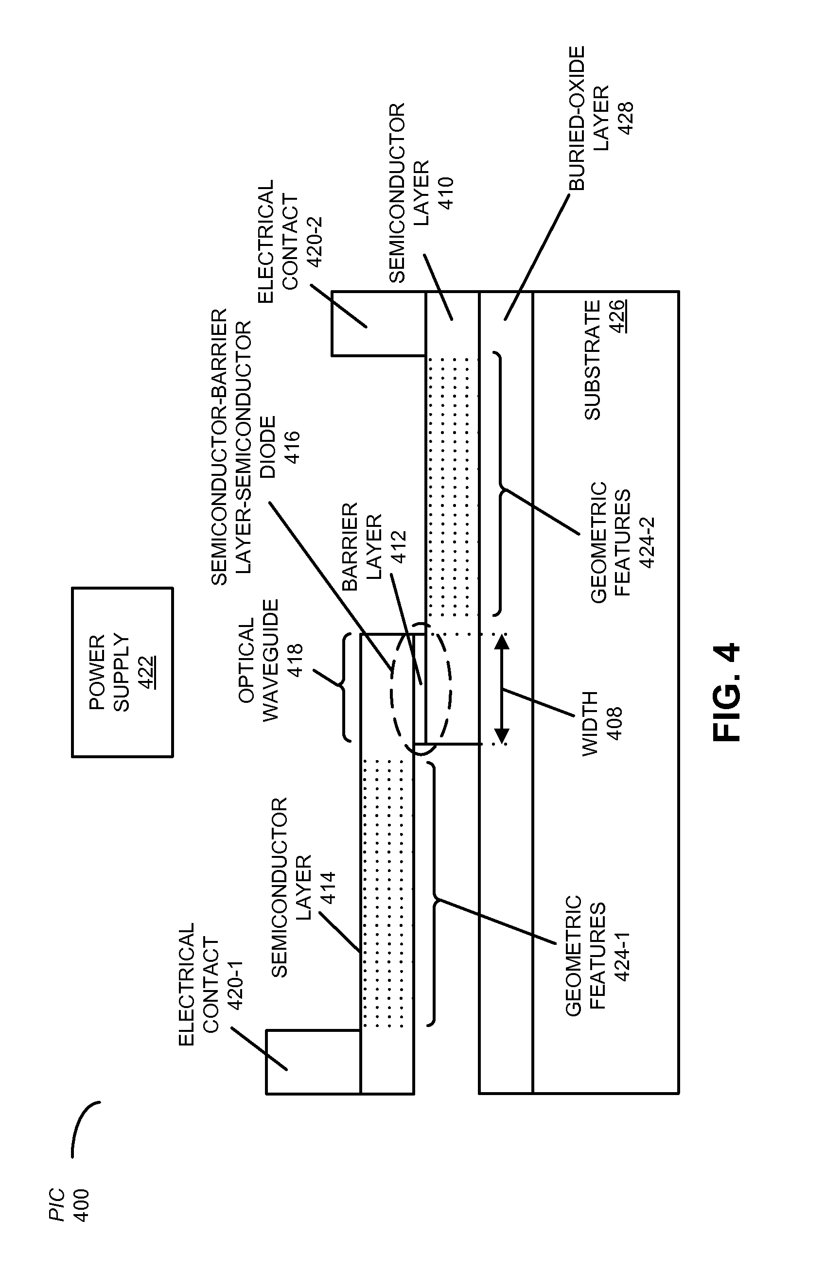
The present disclosure describes an integrated circuit that includes a semiconductor layer and an oxide layer, creating a semiconductor-oxide-semiconductor diode. This diode is included in an optical waveguide that convey an optical signal. The first semiconductor layer and the second semiconductor layer have geometrical features that create a photonic crystal optical waveguide with lower group velocity of light than the first and second semiconductor layers without geometrical features. The integrated circuit can include a substrate, a buried-oxide layer, and the first semiconductor layer. The first semiconductor layer can include silicon and the second semiconductor layer can include polycrystalline silicon. The geometric features can include holes and trenches. The optical waveguide can have two arms that form an optical modulator, such as a Mach-Zehnder interferometer. The system includes the integrated circuit and can convey optical signals. Another integrated circuit includes a first semiconductor layer, a dielectric layer, and a second semiconductor layer, to create a semiconductor-dielectric-semiconductor diode. This diode is also included in an optical waveguide that conveys optical signals. The first and second semiconductor layers have electrical contacts that apply an electric potential across the diode.

Problems solved by technology

This tuning can consume a large amount of electrical power and may require a large area for control circuits, which can significantly increase the cost of the ring-resonator modulators.
While this modulation technique is very efficient, its speed is typically limited to around 1 Gb / s by minority-carrier diffusion.
However, carrier-depletion modulation is often inefficient because it is hard to deplete a lot of charge.
Therefore, phase modulation based on carrier injection or carrier depletion usually cannot simultaneously produce a high-speed (greater than 10 Gb / s), very short MZI (less than 0.3 mm) with a reasonably large ER (greater than 5 dB) under small voltage modulation (less than 2V).
This approach is usually much more efficient than carrier-depletion phase modulation, but is typically less efficient than carrier-injection phase modulation.
However, the diode typically has much higher optical loss (greater than 100 dB / cm) than the PN diodes (less than 10 dB / cm) because of polycrystalline-silicon scattering and absorption.
Consequently, the resulting modulator may have higher optical loss even though its length is much shorter (approximately 6×).
In addition, the diode typically has a very high unit capacitance, which prohibits traveling-wave design and limits modulation speed (because of RC limits associated with the MZI and driver).

Method used


Image

  • Enhanced optical modulation using slow light
  • Enhanced optical modulation using slow light
  • Enhanced optical modulation using slow light

Examples


Embodiment Construction

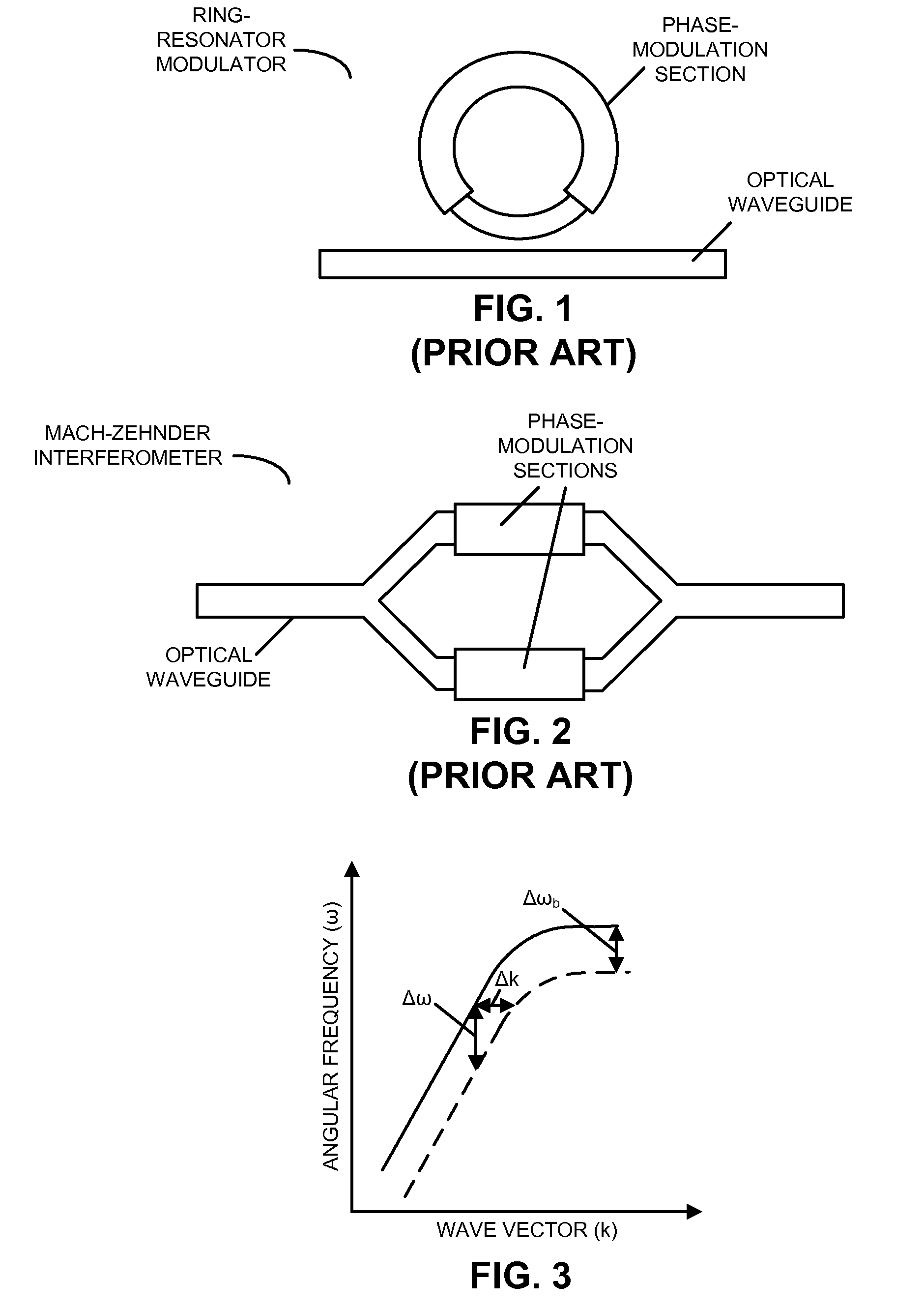
[0029]Embodiments of a photonic integrated circuit (PIC), a system that includes the PIC, and a method for conveying an optical signal are described. This PIC includes a semiconductor-oxide-semiconductor diode in an optical waveguide that conveys an optical signal. Moreover, semiconductor layers in the semiconductor-oxide-semiconductor diode include geometric features (such as a periodic pattern of holes or trenches) that create a lattice-shifted photonic crystal optical waveguide having a group velocity of light that is lower than the group velocity of light in the first semiconductor layer and the second semiconductor layer without the geometric features. The optical waveguide is included in an optical modulator, such as a Mach-Zehnder interferometer (MZI).

[0030]By using slow light to enhance the semiconductor-oxide-semiconductor diode, the performance of the optical modulator can be significantly increased. For example, the effective interaction length and, thus, the modulation e...


PUM


Abstract

A photonic integrated circuit (PIC) is described. This PIC includes a semiconductor-barrier layer-semiconductor diode in an optical waveguide that conveys an optical signal, where the barrier layer is an oxide or a high-k material. Moreover, semiconductor layers in the semiconductor-barrier layer-semiconductor diode may include geometric features (such as a periodic pattern of holes or trenches) that create a lattice-shifted photonic crystal optical waveguide having a group velocity of light that is lower than the group velocity of light in the first semiconductor layer and the second semiconductor layer without the geometric features. The optical waveguide is included in an optical modulator, such as a Mach-Zehnder interferometer (MZI).

Description

GOVERNMENT LICENSE RIGHTS[0001]This invention was made with United States government support under Agreement No. HR0011-08-9-0001 awarded by DARPA. The United States government has certain rights in the invention.BACKGROUND[0002]1. Field[0003]The present disclosure generally relates to the design of photonic integrated circuits (PICs). More specifically, the present disclosure relates to a PIC that includes an optical modulator based on a Mach-Zehnder interferometer (MZI) that uses light slowed by a lattice-shifted photonic crystal optical waveguide to enhance a semiconductor-oxide-semiconductor diode.[0004]2. Related Art[0005]Optical interconnects or links based on silicon photonics have the potential to alleviate inter-chip communication bottlenecks in high-performance computing systems that include a large number of processor chips and memory chips. This is because, relative to electrical interconnects, optical interconnects offer significantly improved: bandwidth, density, power...

Claims


Application Information

Patent Timeline
IPC IPC(8): G02F1/225H04B10/50G02B6/12
CPCG02F1/2257G02F2001/212H04B10/501G02B6/12G02B6/1225G02F2202/32G02F1/212
Inventor LI, GUOLIANGKRISHNAMOORTHY, ASHOK V.ZHENG, XUEZHELUO, YING L.CUNNINGHAM, JOHN E.
Owner ORACLE INT CORP
Learn More