Microelectronic package with stress-tolerant solder bump pattern

Active Publication Date: 2015-04-16
NVIDIA CORP
View PDF1 Cites 10 Cited by
  • Summary
  • Abstract
  • Description
  • Claims
  • Application Information

AI Technical Summary

Benefits of technology

[0008]One advantage of the above-described embodiment is that the reliability of a microelectronic package can be improved. Specifically, the higher mechanical stresses that are caused at the periphery of a microelectronic package by thermal expansion mismatch betw

Problems solved by technology

Consequently, significant mechanical stresses can occur in a 2.5D chip package during operation due to the significant mismatch in coefficient of thermal expansion of the silicon interposer and the organic packaging substrate.
This me

Method used


Image

  • Microelectronic package with stress-tolerant solder bump pattern
  • Microelectronic package with stress-tolerant solder bump pattern
  • Microelectronic package with stress-tolerant solder bump pattern

Examples


Embodiment Construction

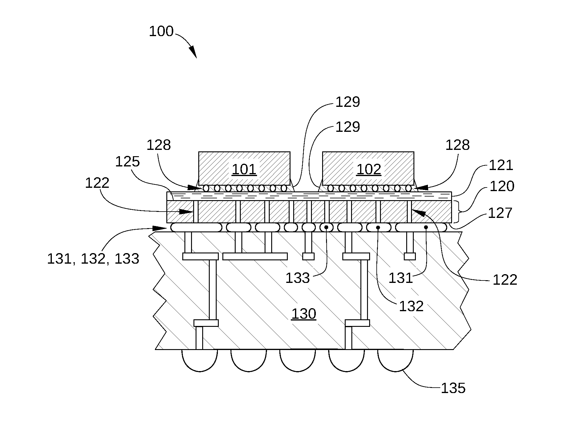
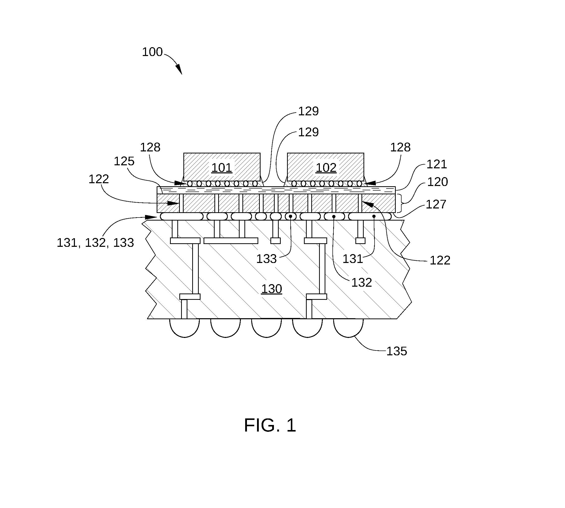
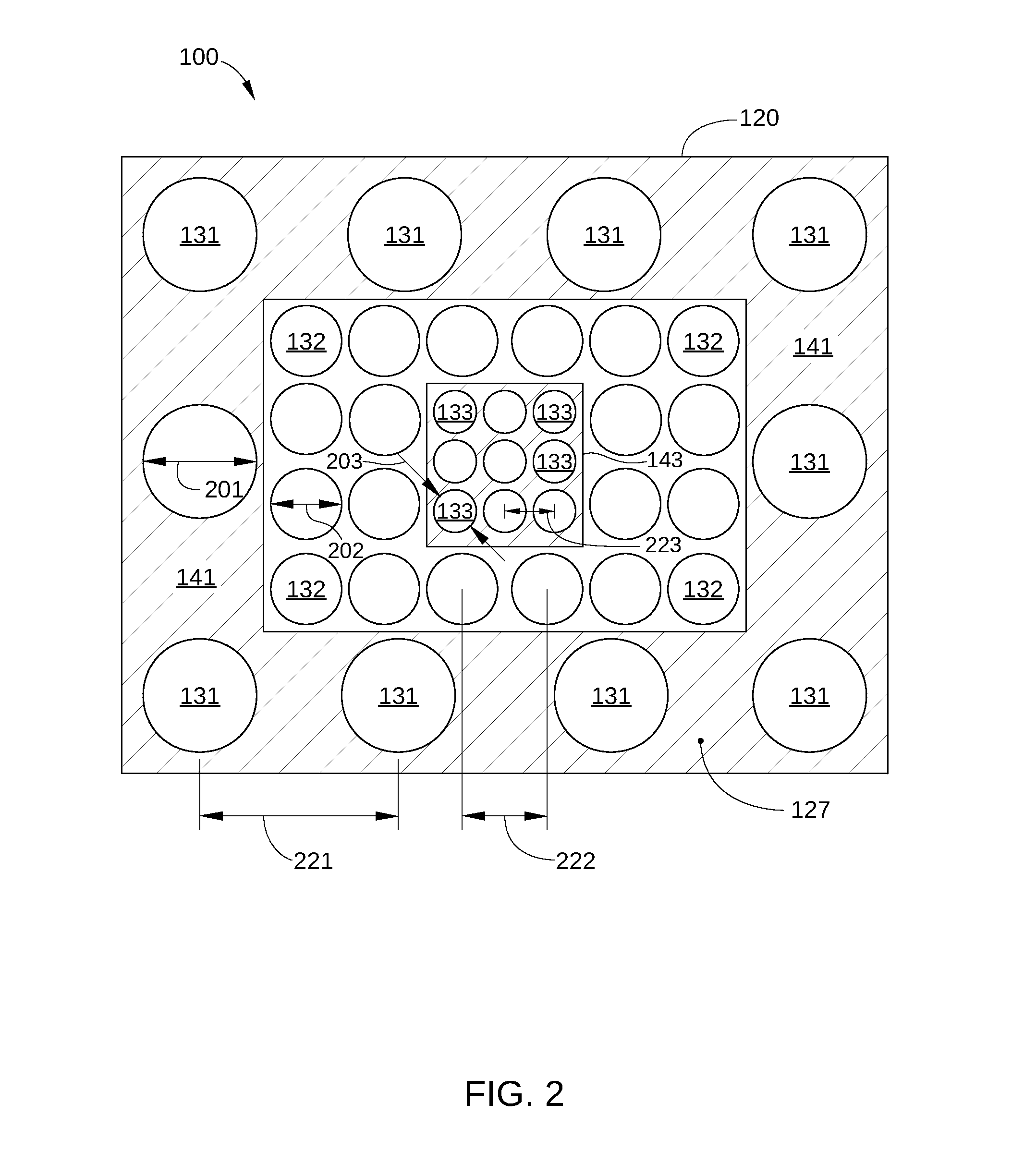
[0016]FIG. 1 is a schematic cross-sectional view of a microelectronic package 100, according to one embodiment of the present invention. Microelectronic package 100 includes integrated circuit (IC) chips 101 and 102, an interposer 120, and a packaging substrate 130. Microelectronic package 100 is configured to electrically and mechanically connect the IC chips 101 and 102 and any other ICs mounted on interposer 120 to a printed circuit board or other mounting substrate (not shown) external to microelectronic package 100. In addition, microelectronic package 100 protects IC chips 101 and 102 from ambient moisture and other contamination and minimizes mechanical shock and stress thereon. For clarity, some elements of IC system 100 are omitted from FIG. 2, such as a heat spreader, over-molding that may be used to encapsulate IC chips 101 and 102, etc.

[0017]Each of IC chips 101 and 102 is a semiconductor chip, such as a central processing unit (CPU), a graphics processing unit (GPU), an...


PUM


Abstract

A microelectronic package includes larger diameter solder bumps and smaller diameter solder bumps for coupling an interposer to a packaging substrate. The larger diameter solder bumps are positioned on a peripheral surface of the interposer and the smaller diameter solder bumps are positioned on a center surface of the interposer. The solder bumps positioned in the peripheral region can more reliably withstand the higher mechanical stresses that occur in this peripheral region during operation of the microelectronic package.

Description

BACKGROUND OF THE INVENTION[0001]1. Field of the Invention[0002]Embodiments of the present invention relate generally to integrated circuit chip packaging and, more specifically, to a microelectronic package with a stress-tolerant solder bump pattern.[0003]2. Description of the Related Art[0004]In the packaging of integrated circuit (IC) chips, the so-called “2.5D” packaging approach has been used for various multi-chip packages, such as field-programmable gate arrays (FPGAs), central processing units (CPUs), or graphics processing units (GPUs) packaged together with one or more dedicated memory chips. In the 2.5D packaging approach, two or more IC chips are mounted on a silicon interposer substrate and electrical connections between the IC chips are formed on the silicon interposer. In addition, the interposer substrate is configured with through-silicon vias (TSVs), which are vertical electrical pathways that pass through the interposer substrate and facilitate electrical connecti...

Claims


Application Information

Patent Timeline
IPC IPC(8): H01L23/00H01L23/12
CPCH01L23/49811H01L24/81H01L24/92H01L24/14H01L23/12H01L23/147H01L23/49816H01L23/49827H01L24/13H01L24/16H01L24/32H01L24/73H01L25/0655H01L2224/131H01L2224/16225H01L2224/32225H01L2224/73204H01L2924/1421H01L2924/1431H01L2924/1434H01L2924/15311H01L2924/157H01L23/49838H01L2924/014H01L2924/00
Inventor ZHANG, LEILEI
Owner NVIDIA CORP
Why Eureka
Try Eureka