Semiconductor module carrying the same

a technology of semiconductors and modules, applied in the field of construction methods, can solve the problems of increasing power, increasing the number of pins assigned to the power supply system, and reducing the mixing noise, so as to ensure the reliability of connection and ensure the stability of power supply

Inactive Publication Date: 2015-04-23
ZYCUBE
View PDF4 Cites 15 Cited by
  • Summary
  • Abstract
  • Description
  • Claims
  • Application Information

AI Technical Summary

Benefits of technology

[0062]According to the present invention, (1) a semiconductor chip or semiconductor device capable of “stable power supplying” can be realized even if the number of the terminals is small due to a terminal configuration with a large permissible current value and so on, (2) the noises which are mixed into the input / output signal system wiring from the power supply system wiring, which has been an issue during high-speed operation, can be reduced, (3) the connection reliability can be ensured due to reduction of the number of the terminals, (4) the area for implementing the semiconductor device(s) or the semiconductor chip(s) can be reduced, and (5) the heat generated in the semiconductor chip can be dissipated effectively.
[0063]By dividing the terminals disposed on the semiconductor chip and disposed them on the first main surface and the second main surface of the semiconductor chip in accordance with the purposes of use, the advantageous effects as described in the preceding paragraph are obtained. The arrangement of the terminals are illustrated specifically as follows:
[0064]The first main surface: the terminal group into which the input signal inflows, the terminal group from which the output signal outflows, the terminal group from which the input signal outflows, and the terminal group into which output signal inflows
[0065]The second main surface: a terminal group into which a power supply current inflows, and a terminal group from which a power supply current outflows
[0066]In the previous paragraph, a capacitor may be disposed between the terminal group into which a supply current inflows and the terminal group from which a supply current outflows, thereby making it possible to absorb transient noises (switching noises) having a high frequency component.
[0067]By disposing an electrical wiring layer on the first main surface of the semiconductor chip and electrically connecting the terminal group of the semiconductor chip, rewiring can be performed.

Problems solved by technology

For this reason, one problem is to develop a semiconductor device capable of “stable power supplying” even with a small number of terminals due to a terminal configuration or the like where allowable current values are large.
In high-speed operation, mixing of noise into the input / output signals from the wiring lines through which large currents flow cause a malfunction.
Therefore, another problem is to reduce the mixing of the noise as small as possible.
Moreover, as described above, the count of pins assigned to the power supply system becomes large with the increasing power.
Therefore, a still another problem is to reduce the pin count, thereby ensuring the connection reliability and reducing the mounting area for mounting the semiconductor device on an application system.

Method used


Image

  • Semiconductor  module carrying the same
  • Semiconductor  module carrying the same
  • Semiconductor  module carrying the same

Examples


first embodiment

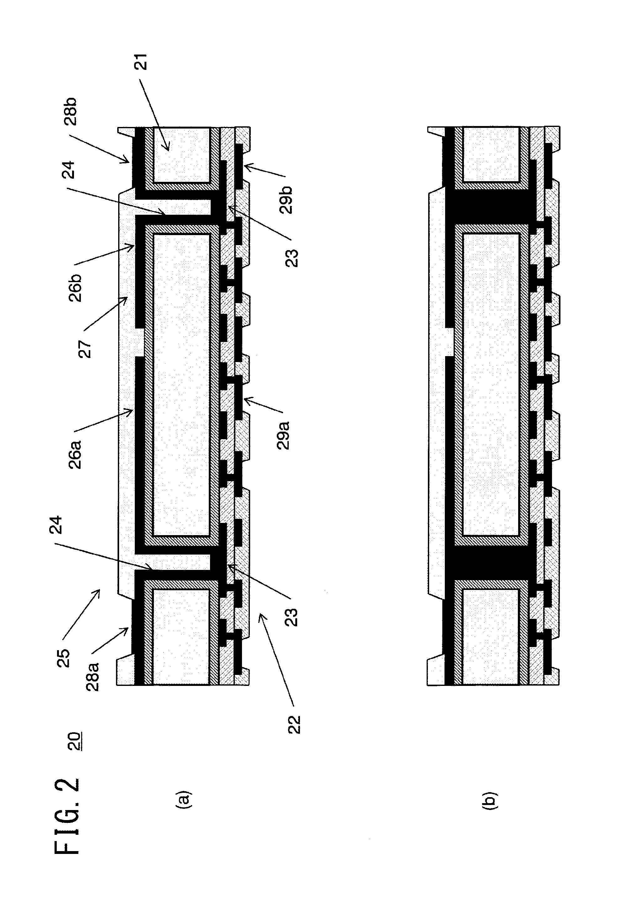
[0094]FIG. 2 is a diagram showing the structure of a semiconductor chip 20 according to a first embodiment of the present invention.

[0095]In FIG. 2(a), 21 denotes a semiconductor substrate, where the lower side of this figure is a first main surface 22. Electronic circuits (not shown) are integrated on the first main surface 22 and a two-layered wiring layer is disposed on the surface thereof. Such the “two-layered wiring layer” is only an example and it may be formed by three or more layers. In this semiconductor substrate, through wirings (which are also referred to as through electrodes) 24 are formed to penetrate through the substrate 21 and to be connected to a designated layer that forms the wiring layer 23. The through wirings 24 are connected to wiring layers 26a and 26b disposed on a second main surface 25 of the semiconductor substrate. In this figure, the number of the wiring layer 26a is one and the number of the wiring layer 26b is also one; however, these numbers are n...

second embodiment

[0106]FIG. 3 is a diagram showing the structure of a semiconductor chip 30 according to the second embodiment of the present invention. In FIG. 3, the same numbers as those shown in FIG. 2 denote the same structural elements.

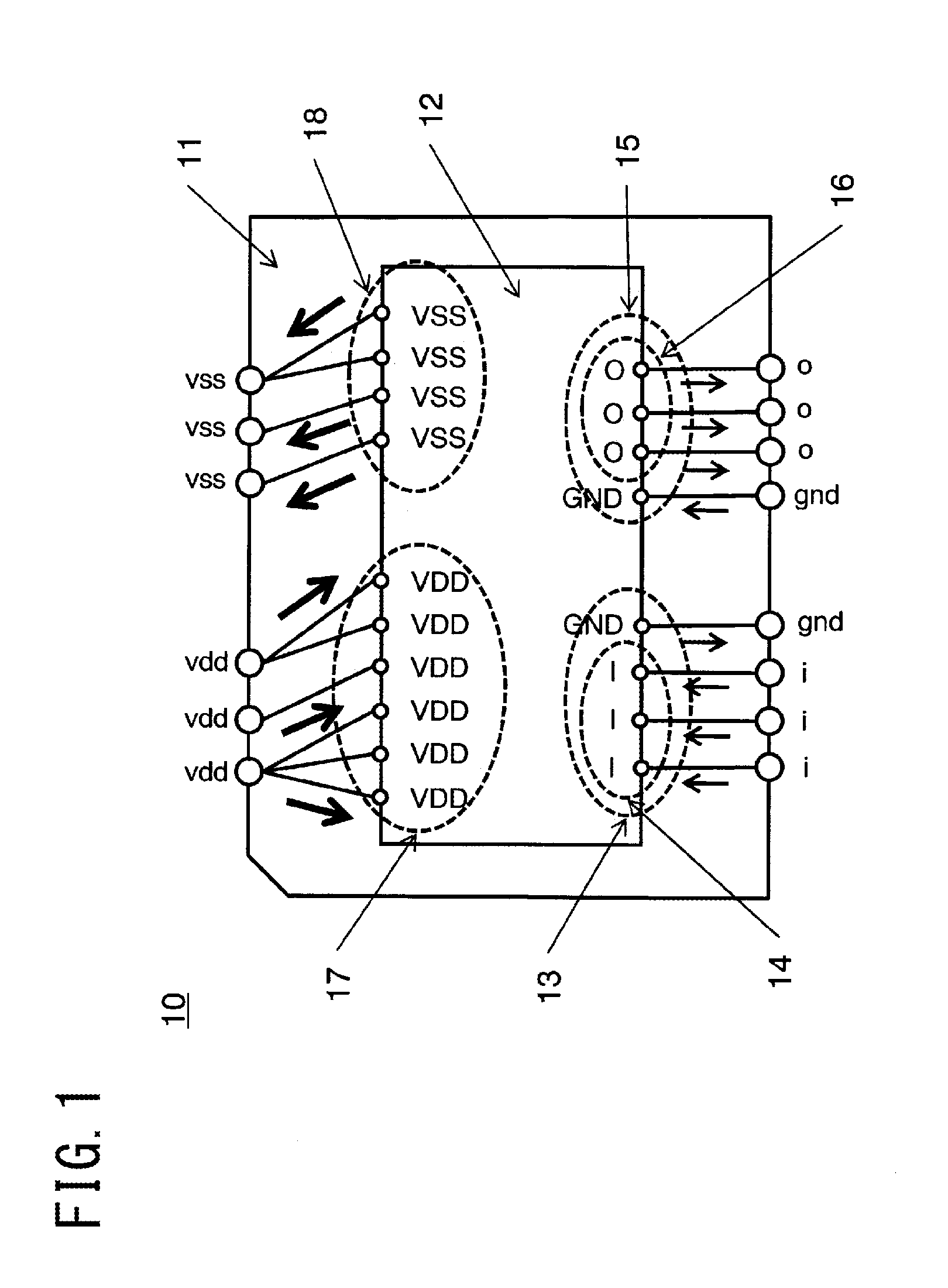
[0107]In FIG. 3(a), 31a and 31b denote through wirings, which are connected to the wiring layer 26a. 31c and 31d also denote through wirings, which are connected to the wiring layer 26b. In FIG. 3(a), the aforementioned through wirings (31a and so on) are arranged at a plurality of positions on the designated wiring layers 23 that constitutes the electronic circuits and the two-layered wiring layer, and are connected to the common wiring layer 26a or 26b. Since the electronic circuits that constitute the semiconductor chip contain the aforementioned wiring layers (23) which are at the same potential, the number of the terminals of this semiconductor chip can be reduced substantially by communizing the aforementioned wiring layers by the wiring layers 26a and 26b...

third embodiment

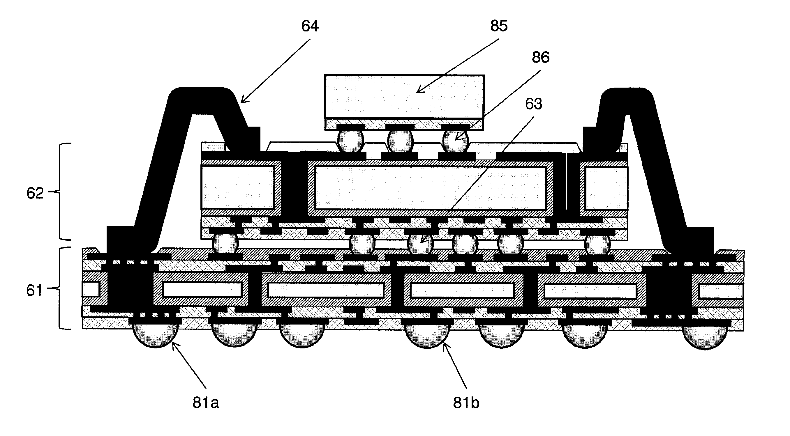
[0111]FIG. 4 is a diagram showing the structure of a semiconductor device according to the third embodiment of the present invention, on which the semiconductor chip 20 shown in FIG. 2 is mounted. In FIG. 4, the same numbers as those shown in FIG. 3 denote the same structural elements. In FIG. 4, 40 denotes the semiconductor devices, and 41 denotes a conductive ball which is disposed in the opening 29a or 29b and which constitutes a ball grid array (BGA). The ball 41 is made of a metal material such as solder (preferably, lead-free solder). In addition, in this figure, a device called “chip size BGA package” is shown as a configuration example of the “semiconductor device”. The semiconductor device of FIG. 4 is similar in structure to the “semiconductor chip” shown in FIG. 2. However, the semiconductor chip of FIG. 2 is in the state of being cut out from a wafer and no protective film for enhancing the environmental resistance is provided. Unlike this, the semiconductor device of FI...


PUM


Abstract

In the conventional high-speed, large-current semiconductor chip, all the electric connecting terminals were placed on one surface of the chip. For this reason, to supply stable supply currents or reduce noises mixed into the signal system from the power supply, many terminals were assigned to supply current inflow terminals and supply current outflow terminals. As a result, there is a problem that the terminal number of a semiconductor device is increased and the mounting area thereof is increased.
The electrical connecting terminals for power supply system and those for signal system are separately placed on both sides of a semiconductor chip. By the configuration to enlarging the permissible current value of a path through which a large current flows, stabilization of feeding supply currents, reduction of noises mixed into signal systems, reduction of mounting areas due to pin count reduction, and increase of heat dissipation effects can be realized even with a decreased pin count. Moreover, by the semiconductor module on which the semiconductor chip is mounted, stable characteristics can be realized even in high-speed operation necessitating large currents.

Description

TECHNICAL FIELD[0001]The present invention relates to a construction method of a high pin-count or high-power semiconductor device. The present invention is also relates to a construction method of a semiconductor module carrying this semiconductor device.BACKGROUND ART[0002]In recent years, technological advances in semiconductor devices are large, and semiconductor devices have been widely used in industrial and consumer equipment. As a result, technological advances has contributed significantly to size reduction, weight reduction, price lowering, and performance advancement of equipment and systems carrying semiconductor devices. On the other hand, the request to improving semiconductor devices is not stopped and as a result, higher integration, higher speed, and more sophistication as well as miniaturization are expected. If these requirements are met, the pin count and electric power of semiconductor devices will be necessarily increased. In addition, if the high power and hig...

Claims


Application Information

Patent Timeline
Patent Type & Authority Applications(United States)
IPC IPC(8): H01L23/00H01L49/02
CPCH01L24/17H01L28/60H01L2924/1205H01L2924/14H01L24/49H01L23/481H01L23/49816H01L23/49822H01L23/5223H01L23/5286H01L2224/16225H01L2924/15311H01L2924/19107H01L23/49833H01L2224/73204H01L2224/73253H01L2924/19105H01L23/642H01L25/0657H01L25/16H01L2225/0651H01L2225/06517H01L2225/06513H01L2225/06558H01L2224/48227H01L2224/48472H01L2224/45015H01L2224/05569H01L2224/16147H01L2224/02379H01L2224/02371H01L24/02H01L24/05H01L24/13H01L24/16H01L24/45H01L24/48H01L24/73H01L2224/02331H01L2224/02372H01L2224/02381H01L2224/0239H01L2224/0401H01L2224/04042H01L2224/05624H01L2224/131H01L2224/16145H01L2224/48096H01L2224/49113H01L2224/49175H01L2224/73207H01L2224/73257H01L2924/00014H01L2924/2075H01L2924/20757H01L2924/20756H01L2924/20758H01L2924/20759H01L2924/2076H01L2924/20754H01L2924/20755H01L2924/01029H01L2924/014H01L2924/00015H01L2224/45099H01L2924/00H01L2224/48095
Inventor NAKAMURA, HIROFUMI
Owner ZYCUBE
Why Eureka
Try Eureka