
MEMS Device with Outgassing Shield

Active Publication Date: 2015-04-30
ANALOG DEVICES INC
View PDF8 Cites 22 Cited by
  • Summary
  • Abstract
  • Description
  • Claims
  • Application Information

AI Technical Summary

Benefits of technology

The patent describes a capped micromachined device that includes a MEMS structure and a cap with electrical conductors. The device has a MEMS chamber enclosed by the cap and a shield layer, and an interconnection chamber that is isolated from the MEMS chamber. The interconnection chamber includes an interconnection structure that electrically couples the two electrical conductors. The device also includes a first isolation wall and a second isolation wall to provide complete outgassing protection. The technical effect of this invention is to provide a capped micromachined device with improved protection and reliability.

Problems solved by technology

Such gasses, once released into the inside of the device's hermetically sealed cavity, can cause much higher sealed pressure than desired, and adversely impact the performance of the MEMS device.
For example, such gasses may cause an accelerometer or gyroscope to fail to meet their respective specifications.
Even for devices that do not require a low pressure cavity environment within a cavity, this outgas can cause the pressure to be at or about 1 atmosphere, so the basic Q measurement for hermeticity screening may not be possible.

Method used


Image

  • MEMS Device with Outgassing Shield
  • MEMS Device with Outgassing Shield
  • MEMS Device with Outgassing Shield

Examples


first embodiment

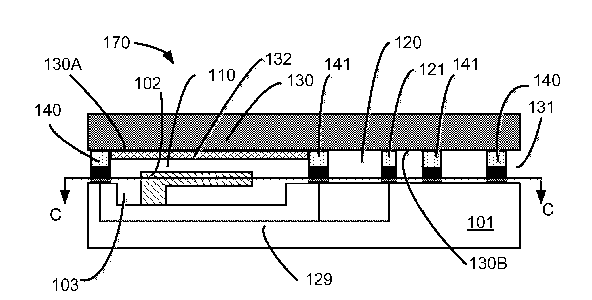
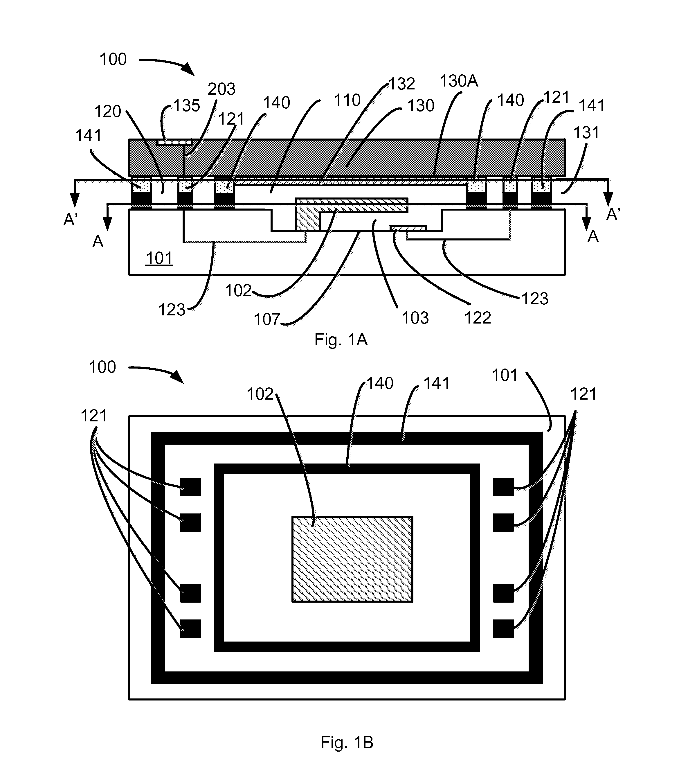
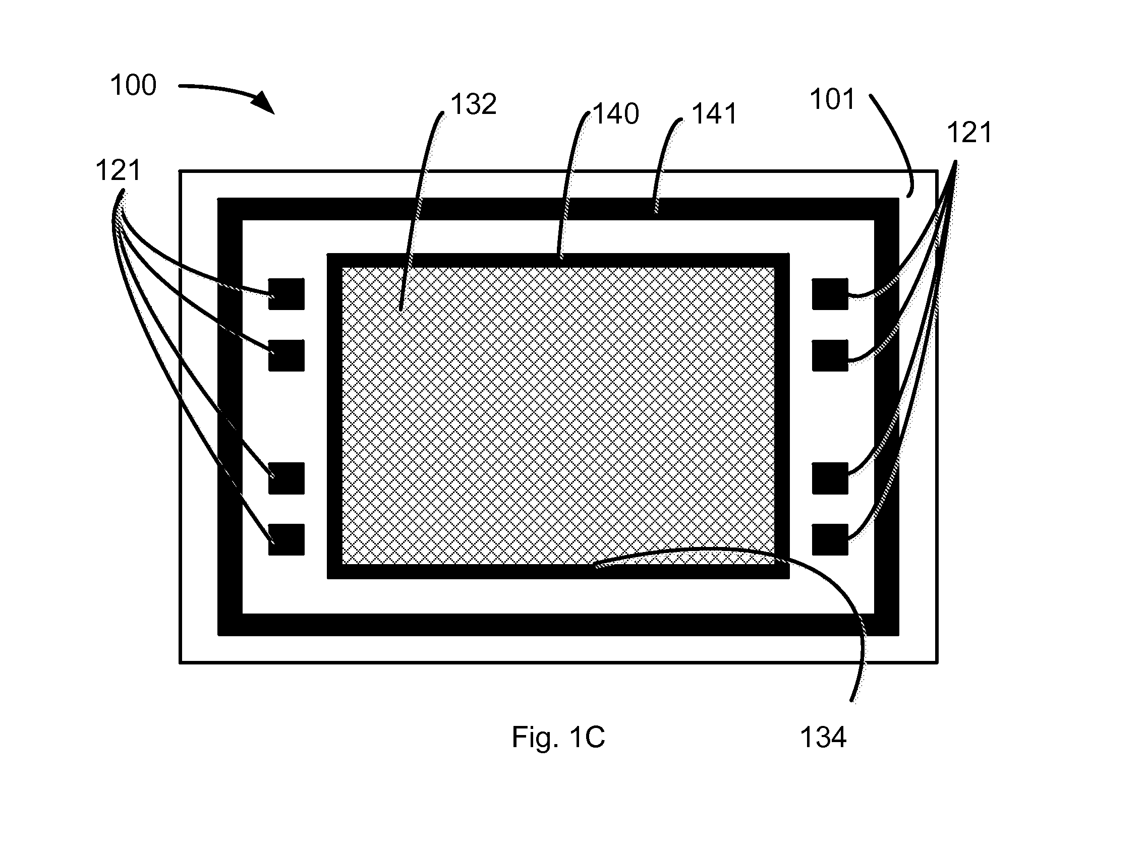
[0005]In a first embodiment, a capped micromachined device includes a MEMS structure in a MEMS chamber, and a cap that includes an outgassing shield configured to prevent outgassing from the cap from entering the MEMS chamber. In particular, the capped micromachined device includes a substrate having a MEMS structure suspended from a substrate, and at least a first electrical conductor coupled to the MEMS structure and to the cap. In various embodiments, the MEMS structure may be one of an accelerometer beam, a gyroscope structure, and a switch arm, to name but a few examples.

[0006]The device also includes a cap suspended parallel to the substrate and separated from the substrate by a capping gap. The cap includes at least a second electrical conductor, such as doped conductive lines or metal interconnections on the surface of, or within, the cap. In some embodiments, the cap is an integrated circuit including a plurality of active semiconductor devices. Indeed, in some embodiments,...

second embodiment

[0025]FIGS. 1D and 1E schematically illustrate a capped MEMS device having a MEMS chamber that is hermetically isolated from interconnections;

third embodiment

[0026]FIGS. 1F and 1G and 1H schematically illustrate a capped MEMS device having a MEMS chamber that is hermetically isolated from interconnections;

[0027]FIG. 2A schematically illustrates an embodiment of a capped MEMS device having a MEMS chamber that is hermetically isolated from interconnections and through-silicon vias and solder balls;

[0028]FIGS. 2B and 2C schematically illustrate an alternate embodiment of a capped MEMS device having a MEMS chamber that is hermetically isolated from interconnections and having solder balls;

[0029]FIG. 3A is a flow chart that schematically illustrates an embodiment of a method of fabricating a capped MEMS device having a MEMS chamber that is hermetically isolated from interconnections;

[0030]FIG. 3B schematically illustrates various portions of a capped MEMS device corresponding to the flow chart of FIG. 3A;

[0031]FIG. 4 is a flow chart that schematically illustrates an embodiment of a method of fabricating a cap;

[0032]FIGS. 5A-5F schematically i...


PUM

PropertyMeasurementUnit
Electrical conductoraaaaaaaaaa

Abstract

A capped micromachined device has a movable micromachined structure in a first hermetic chamber and one or more interconnections in a second hermetic chamber that is hermetically isolated from the first hermetic chamber, and a barrier layer on its cap where the cap faces the first hermetic chamber, such that the first hermetic chamber is isolated from outgassing from the cap.

Description

TECHNICAL FIELD[0001]The present invention relates to micromachined (“MEMS”) devices, and more particularly to packaging for MEMS devices.BACKGROUND ART[0002]It is known in the prior art to hermetically cap a MEMS device, and to make electrical connections between the MEMS device and a related integrated circuit via wire bonds outside of the hermetic cap.[0003]It is also known to attach the related integrated circuit to the substrate of the MEMS device via a seal ring, such that the related integrated circuit acts as a cap to hermetically seal the MEMS device in a cavity. Such devices make the electrical connections between the MEMS device and the capping integrated circuit by providing electrically conductive interconnections extending directly between the substrate and related integrated circuit within the hermetic cavity.[0004]However, it is known that typical backend films used for inter-metal isolation and top passivation in integrated circuits, such as PECVD oxide and PECVD ni...

Claims


Application Information

Patent Timeline
IPC IPC(8): B81B7/00B81C3/00B81C1/00B81B3/00
CPCB81B7/0035B81C1/00293B81C3/001B81B3/0094B81B7/0041B81B2201/0235B81B2207/012B81B2207/095B81C2203/019
Inventor CHEN, LINUNAN, THOMAS KIERANYANG, KUANG L.
Owner ANALOG DEVICES INC
Learn More