Three Dimensional Nonvolatile Memory Cell Structure with Upper Body Connection

Active Publication Date: 2015-05-14
CONVERSANT INTPROP MANAGEMENT INC
View PDF5 Cites 36 Cited by
  • Summary
  • Abstract
  • Description
  • Claims
  • Application Information

AI Technical Summary

Benefits of technology

The present invention relates to nonvolatile memory devices, particularly flash memory, and methods for manufacturing them. The technical effects of the invention include reducing the size of memory cells and increasing memory capacity per unit area by designing and fabricating vertical NAND flash memory cell strings. The invention also addresses challenges associated with designing and fabricating vertical NAND flash memory devices, such as limitations imposed by photolithography tools. The drawings include various cross-sectional views of the vertical NAND flash memory cell structure, including a simplified circuit schematic representation, cross-sectional views of the NAND flash memory cell array, and a plan view of the upper body connection layer. The invention aims to improve the performance and cost-effectiveness of nonvolatile memory devices, particularly flash memory, for use in consumer electronics and other applications.

Problems solved by technology

But as fabrication process limitations (for example, limitations imposed by photolithography tools) limit the ability to reduce physical transistor sizes, there have been structural and / or design schemes proposed to increase memory density, such as, for example, stacking NAND cells in a direction perpendicular to the chip surface, thereby reducing the effective chip area per data bit without requiring shrinkage of the physical cell transistor size.
However, there continue to be challenges associated with designing, fabricating, and operating vertical NAND flash memory devices.

Method used


Image

  • Three Dimensional Nonvolatile Memory Cell Structure with Upper Body Connection
  • Three Dimensional Nonvolatile Memory Cell Structure with Upper Body Connection
  • Three Dimensional Nonvolatile Memory Cell Structure with Upper Body Connection

Examples


Embodiment Construction

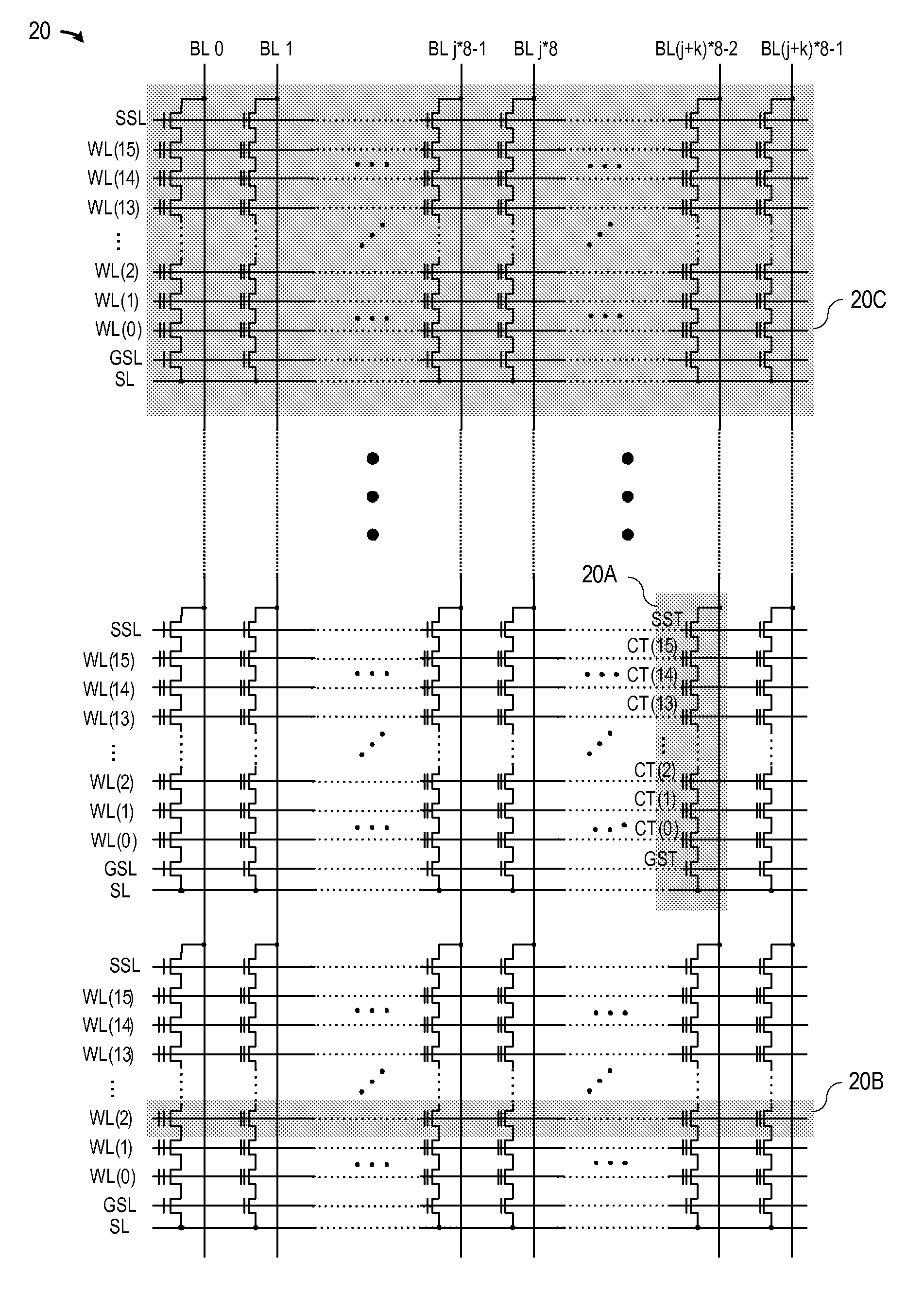
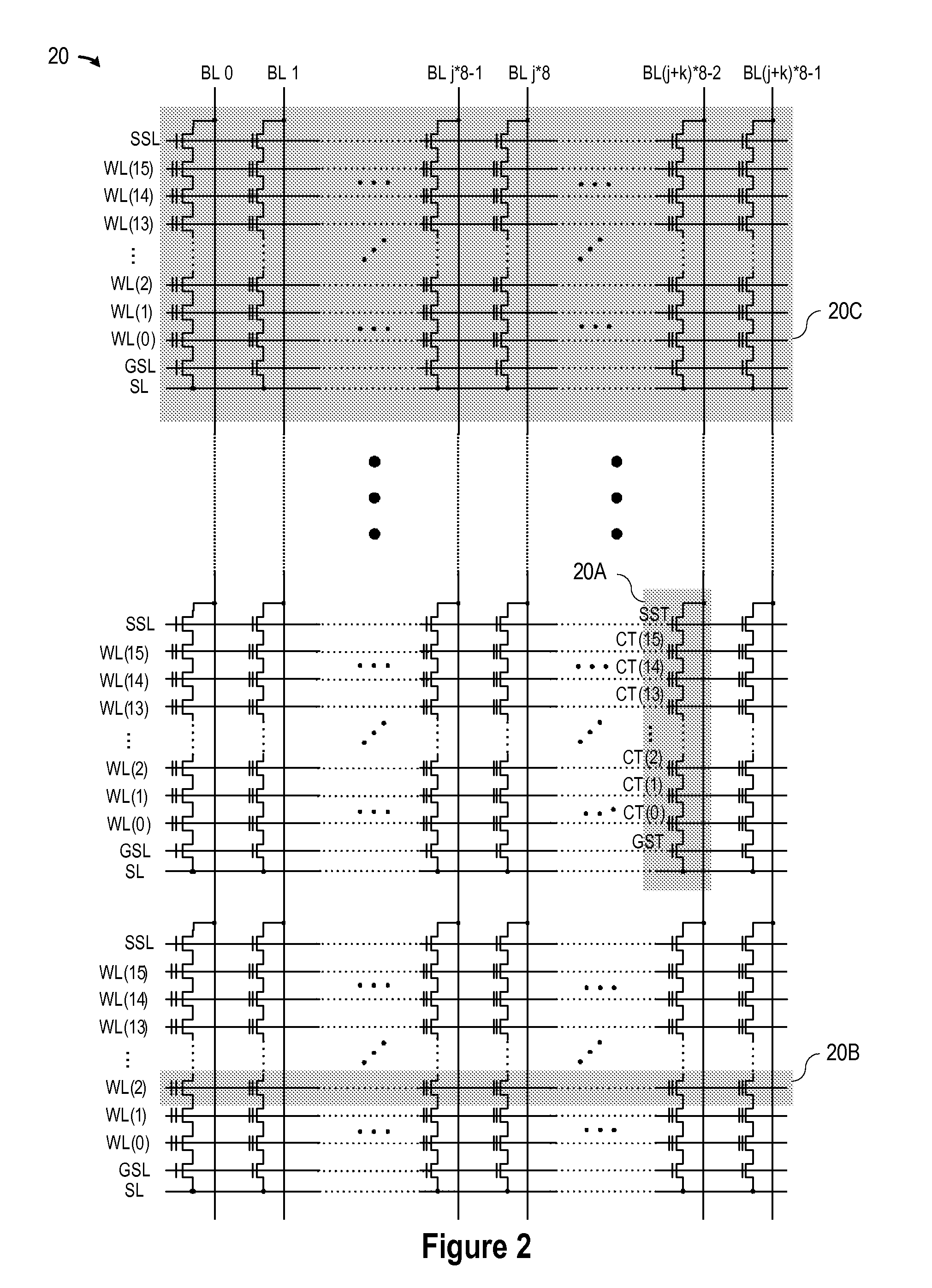
[0023]In a three-dimensional vertical channel NAND flash memory device, a stacked memory architecture and cell array structure are provided with upper connection lines formed with semiconductor strips or in a single semiconductor layer. The upper connection lines include n-type bit line nodes for connection to vertical string channels through horizontal string body portions. The upper connection lines also include p-type body nodes for direct electrical connection to vertical string bodies through horizontal string body portions to provide direct charging through a common body node during erase operations. By connecting the flash cell strings between the upper connection lines and an n-type source line formed in the substrate, the transistors on each string may include a plurality of series-connected transistors, including a string select transistor having a drain which is electrically connected to an n-type bit line node of the upper connection line and a source which is connected ...


PUM


Abstract

A three-dimensional integrated circuit non-volatile memory array includes a memory array of vertical channel NAND flash strings connected between a substrate source line and upper layer connection lines which each include n-type drain regions and p-type body line contact regions alternately disposed on each side of undoped or lightly doped string body regions so that each NAND flash string includes a vertical string body portion connected to a horizontal string body portion formed from the string body regions of the upper body connection lines.

Description

BACKGROUND OF THE INVENTION[0001]1. Field of the Invention[0002]The present invention is directed in general to integrated circuit devices and methods for manufacturing same. In one aspect, the present invention relates to nonvolatile memory devices, such as NAND flash memory and other types of flash memory.[0003]2. Description of the Related Art[0004]With the increasing demand for nonvolatile data storage in consumer electronics having mass storage, such as video or audio players, digital cameras, and other computerized devices, there continues to be interest in having nonvolatile memory devices progress over time towards having smaller sizes, larger memory capacity, and improved performance. Flash memory is a commonly used type of nonvolatile memory which can take the form of memory cards or USB type memory sticks, each having at least one memory device and a memory controller formed therein. For example, the need to reduce manufacturing costs per data bit is driving the NAND flas...

Claims


Application Information

Patent Timeline
IPC IPC(8): H01L27/115G11C16/26G11C16/14
CPCH01L27/11556G11C16/14H01L27/11582H01L27/11524H01L27/1157G11C16/26H01L29/7926G11C16/0408G11C16/0483H10B43/35H10B43/27H10B41/27H10B41/35
Inventor RHIE, HYOUNG SEUB
Owner CONVERSANT INTPROP MANAGEMENT INC
Why Eureka
Try Eureka