Eureka AIR delivers breakthrough ideas for toughest innovation challenges, trusted by R&D personnel around the world.

High voltage junction field effect transistor

Active Publication Date: 2015-05-21
CSMC TECH FAB2 CO LTD
View PDF3 Cites 21 Cited by
  • Summary
  • Abstract
  • Description
  • Claims
  • Application Information

AI Technical Summary

Benefits of technology

The present invention provides a high voltage JFET that uses RESURF principle to enhance its breakdown voltage. By arranging the channel on the epitaxial layer, and controlling the implantation conditions of the channel implantation layer, the pinch-off voltage of the high voltage JFET can be adjusted. The technology for producing the high voltage JFET is compatible with conventional CMOS / LDMOS integrated circuit producing technology, making it suitable for high voltage semiconductor integrated circuit producing technology.

Problems solved by technology

So the breakdown voltage of the JFET cannot be improved either by a filed electrode or by other types.
So, the conventional JFET is limited by PN junction, and the breakdown voltage is about 20˜30 volts, thereby limiting an application of JFET in high voltage field.

Method used


Image

  • High voltage junction field effect transistor
  • High voltage junction field effect transistor
  • High voltage junction field effect transistor

Examples


embodiment one

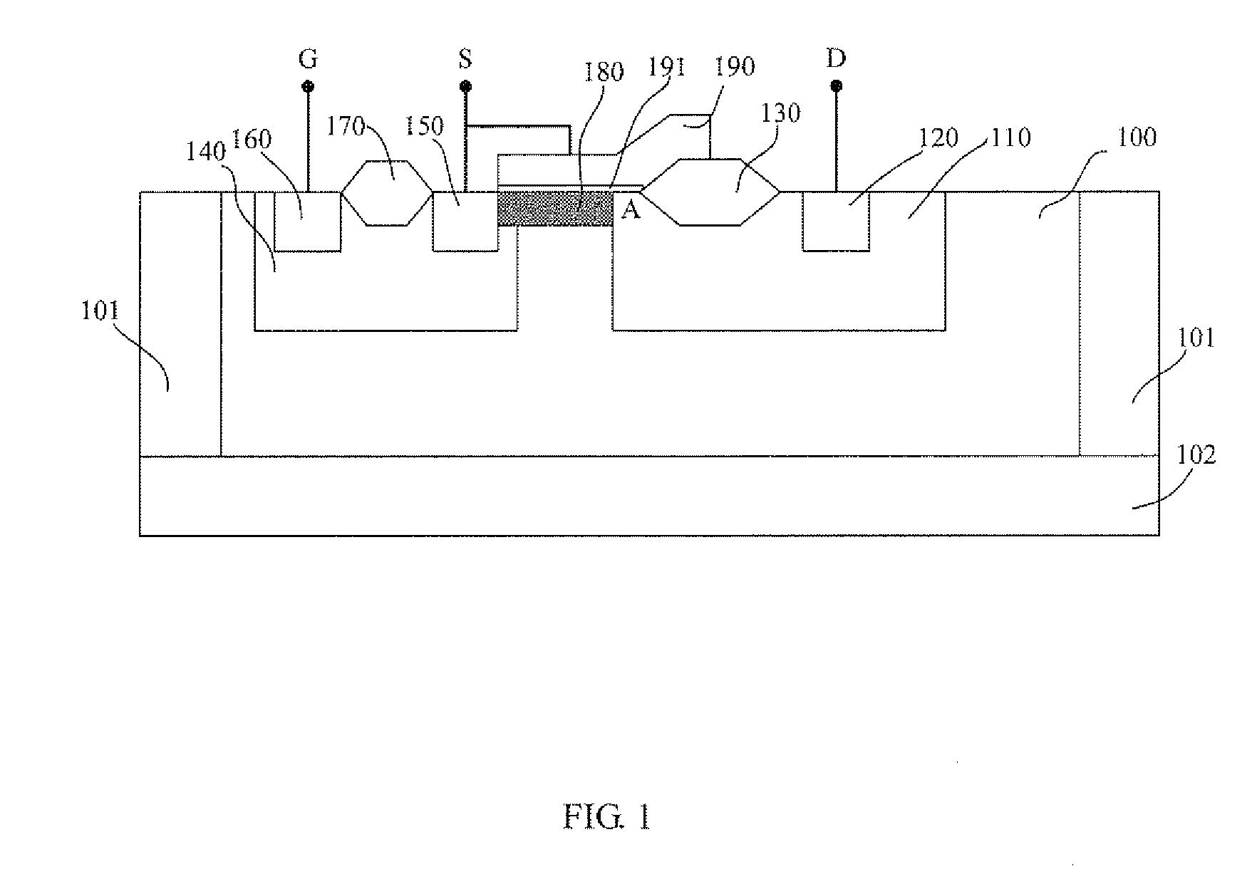
[0047]Referring to FIG. 1, a high voltage JFET includes: a semiconductor substrate provided with a first conductivity type epitaxial layer 100; a second conductivity type drift region 110 located on the first conductivity type epitaxial layer 100; a second conductivity type drain heavily doped region 120 located in the second conductivity type drift region 110; a drain terminal oxygen region 130 located on the second conductivity type drift region 110 and at a side of the second conductivity type drain heavily doped region 120; a first conductivity type well region 140 located at a side of the second conductivity type drift region 110 and isolated from the second conductivity type drift region 110 by the first conductivity type epitaxial layer 100; a second conductivity type source heavily doped region 150 and a first conductivity type gate heavily doped region 160 located on the first conductivity type well region 140, a gate source terminal oxygen region 170 located between the se...

embodiment two

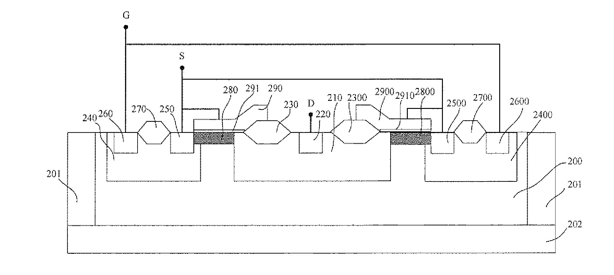
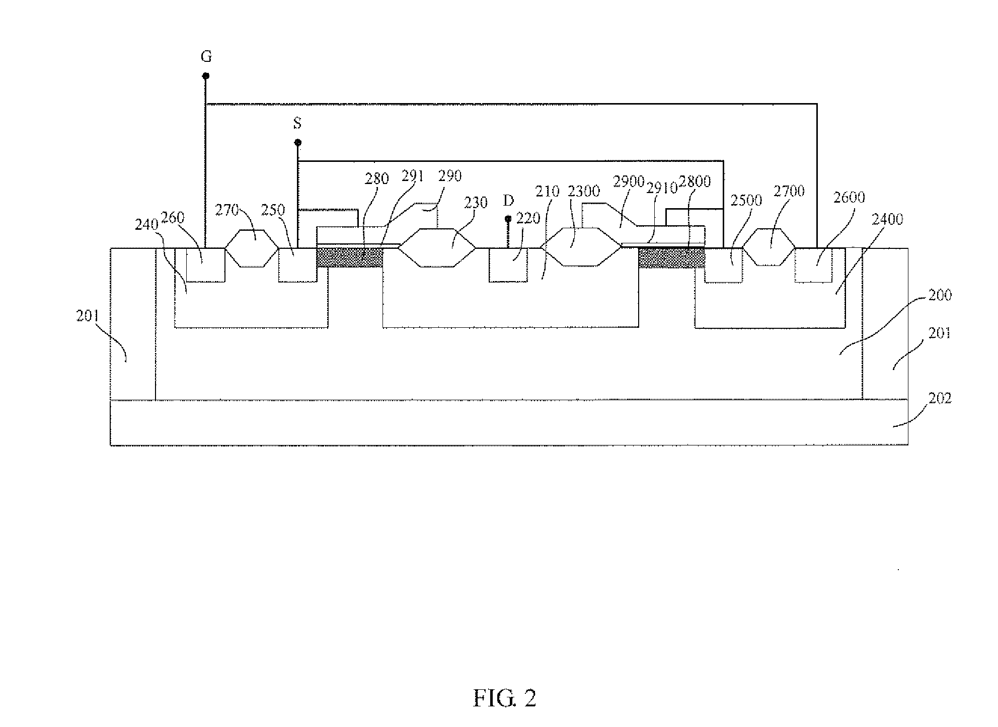
[0053]referring to FIG. 2, another one high voltage JFET includes: a semiconductor substrate provided with a first conductivity type epitaxial layer 200; a second conductivity type drift region 210 located on the first conductivity type epitaxial layer 200; a second conductivity type drain heavily doped region 220 located in the second conductivity type drift region 210; a first drain terminal oxygen region 230 and a second drain terminal oxygen region 2300 located at opposite sides of the second conductivity type drain heavily doped region 220, and both the oxygen regions 230, 2300 being positioned on the second conductivity type drift region 210; a first first conductivity type well region 240 and a second first conductivity type well region 2400 located at opposite sides of the second conductivity type drift region 210, and both the well regions 240, 2400 being isolated from the second conductivity type drift region 210 by the first conductivity type epitaxial layer 200; a first ...


PUM


Abstract

The present invention discloses a high voltage JFET. The high voltage JFET includes a second conductivity type drift region located on the first conductivity type epitaxial layer; a second conductivity type drain heavily doped region located in the second conductivity type drift region; a drain terminal oxygen region located on the second conductivity type drift region and at a side of the second conductivity type drain heavily doped region; a first conductivity type well region located at a side of the second conductivity type drift region; a second conductivity type source heavily doped region and a first conductivity type gate heavily doped region located on the first conductivity type well region, and a gate source terminal oxygen region; a second conductivity type channel layer located between the second conductivity type source heavily doped region and the second conductivity type drift region; a dielectric layer and a field electrode plate located on the second conductivity type channel layer. Wherein a drain electrode electrically is led out from the second conductivity type drain heavily doped region; a source electrode electrically is led out from a connection of the field electrode plate and the second conductivity type source heavily doped region; and a gate electrode electrically is led out from the first conductivity type gate heavily doped region. The transistor has a high breakdown voltage and easy to be integrated.

Description

FIELD OF THE INVENTION[0001]The present invention relates to a device structure of a field effect transistor, and more particularly, relates to a JFET (Junction Field Effect Transistor) applied in high voltage, which belongs to a field of semiconductor producing.BACKGROUND OF THE INVENTION[0002]Field effect transistors are widely employed to design various simulation circuits, for example, applied to an amplifier circuit, a biasing circuit or a step-down circuit, a starting circuit, or a variable resistance, and so on. As an emerging demand for high voltage devices, how to improve breakdown voltage of various kinds of field effect transistors has become a design target of high voltage field effect transistor.[0003]For MOSFET (Metal-Oxide-Semiconductor Field Effect Transistor), a DMOS (Double-diffused. MOS) employing a planar diffusion technology is provided with characteristics such as a high current drive capacity, a low on-resistance, and a high breakdown voltage, such that DMOS i...

Claims


Application Information

Patent Timeline
IPC IPC(8): H01L29/808H01L29/40H01L29/10
CPCH01L29/808H01L29/402H01L29/1058H01L29/0843H01L29/1066H01L29/0653
Inventor HAN, GUANGTAO
Owner CSMC TECH FAB2 CO LTD
Why Eureka
Eureka Blog
Learn More