Substrate Tuning System and Method Using Optical Projection

a technology of optical projection and substrate, applied in the field of substrate patterning, can solve the problems of insufficient preventive measures of semiconductor fabrication processes, process of developing and producing semiconductors, etc., and achieve the effects of improving temperature uniformity across the surface of the substrate, reducing defectivity, and increasing temperature uniformity

Active Publication Date: 2015-05-28
TOKYO ELECTRON LTD
View PDF11 Cites 9 Cited by
  • Summary
  • Abstract
  • Description
  • Claims
  • Application Information

AI Technical Summary

Benefits of technology

[0005]Techniques disclosed herein, however, can provide temperature uniformity to within about 0.02 degrees Celsius. Such an increase in temperature uniformity reduces defectivity and enables continued scaling of semiconductor devices.
[0006]Techniques herein include systems and methods that provide a spatially-controlled projection of light or electromagnetic (EM) radiation onto a substrate. Combining such spatial light projection with hot plate heating can achieve significant improvements in temperature uniformity across a surface of a substrate. A wavelength of 400-700 nm light, Ultra Violet Light (UV), infrared light, or any wavelength directed at an object can produce heat on the impact site of projected light. As total energy increases at a specific point on a substrate, a temperature of that point will increase until it reaches a steady state value. The steady state temperature on a substrate can be varied and controlled using different intensities and wavelengths within the range of a light source, such as a lamp. A given projected image can comprise multiple intensities and various wavelengths, which can be set to change and maintain many different steady state conditions on multiple substrates simultaneously. In other words, a substrate holder heat source in combination with a projected light image of a particular spatial heat signature can increase temperature uniformity across the surface of a substrate.
[0007]In one embodiment a camera / detector and a projector are directed at a substrate. The projector illuminates the substrate with light (at least a portion is illuminated), which can be based on a heat signature detected from an infrared detecting camera. The substrate can then have a modulated temperature with high spatial resolution with any number of light patterns and intensities. With the camera (or sensory array / sensor mechanism) detecting a heat signature, a corresponding pixelated image can be projected onto a substrate surface to modify surface temperature. Thus, a heat signature can be controlled by pixel, that is, controlled by spot or grid point location on the substrate surface. The projected image can be tailored to specific results desired. For example, if temperature uniformity is desired, then the projected image can be an inverse of the heat signature to essentially heat cold areas and / or cool or maintain warm areas. Thus, a combination of fine and coarse control for a hotplate can provide significantly better uniformity. Because light is heat, areas that need spatial temperature adjustment can be irradiated with an amount of light. Because light can alter material properties of certain materials (such as photoresists), existing exposures can be augmented to be biases up or down. Thus, an additional embodiment includes tuning film properties using a pixel-based projected light pattern.
[0008]Such systems and methods enable semiconductor manufacturers to meet design demands. Design specifications for semiconductor manufacturing limit the process of developing and producing semiconductors by forcing a set of parameters onto the engineer that current technology cannot avoid. One of these design specifications is related to the baking step of semiconductor production. When a substrate is baked it is baked uniformly at a particular temperature and for an amount of time. Being able to replace the constant of uniform temperature with variable temperature gives a process controller more flexibility and increases efficiency of semiconductor production.

Problems solved by technology

Unfortunately, having a tolerance or temperature fluctuation of 0.1° C. can be insufficient to prevent defects in semiconductor fabrication processes.
Design specifications for semiconductor manufacturing limit the process of developing and producing semiconductors by forcing a set of parameters onto the engineer that current technology cannot avoid.

Method used


Image

  • Substrate Tuning System and Method Using Optical Projection
  • Substrate Tuning System and Method Using Optical Projection
  • Substrate Tuning System and Method Using Optical Projection

Examples


Embodiment Construction

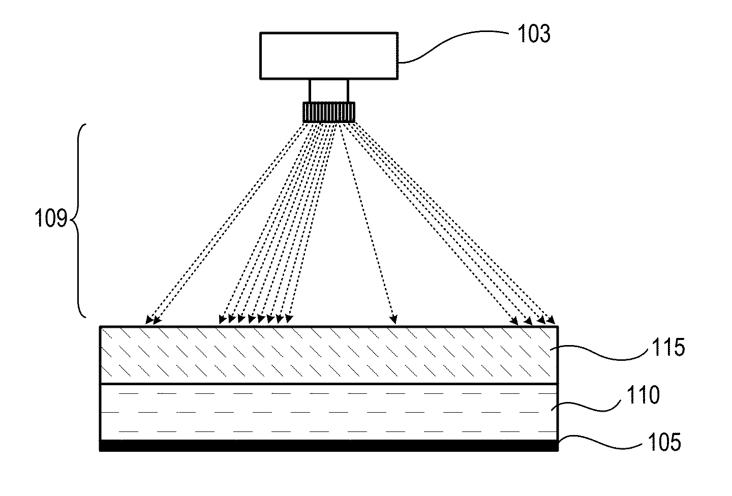
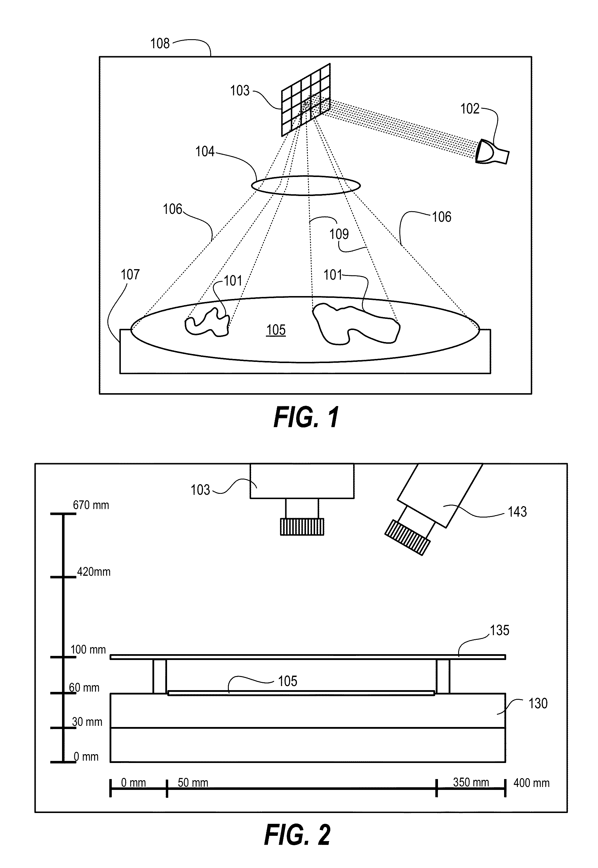
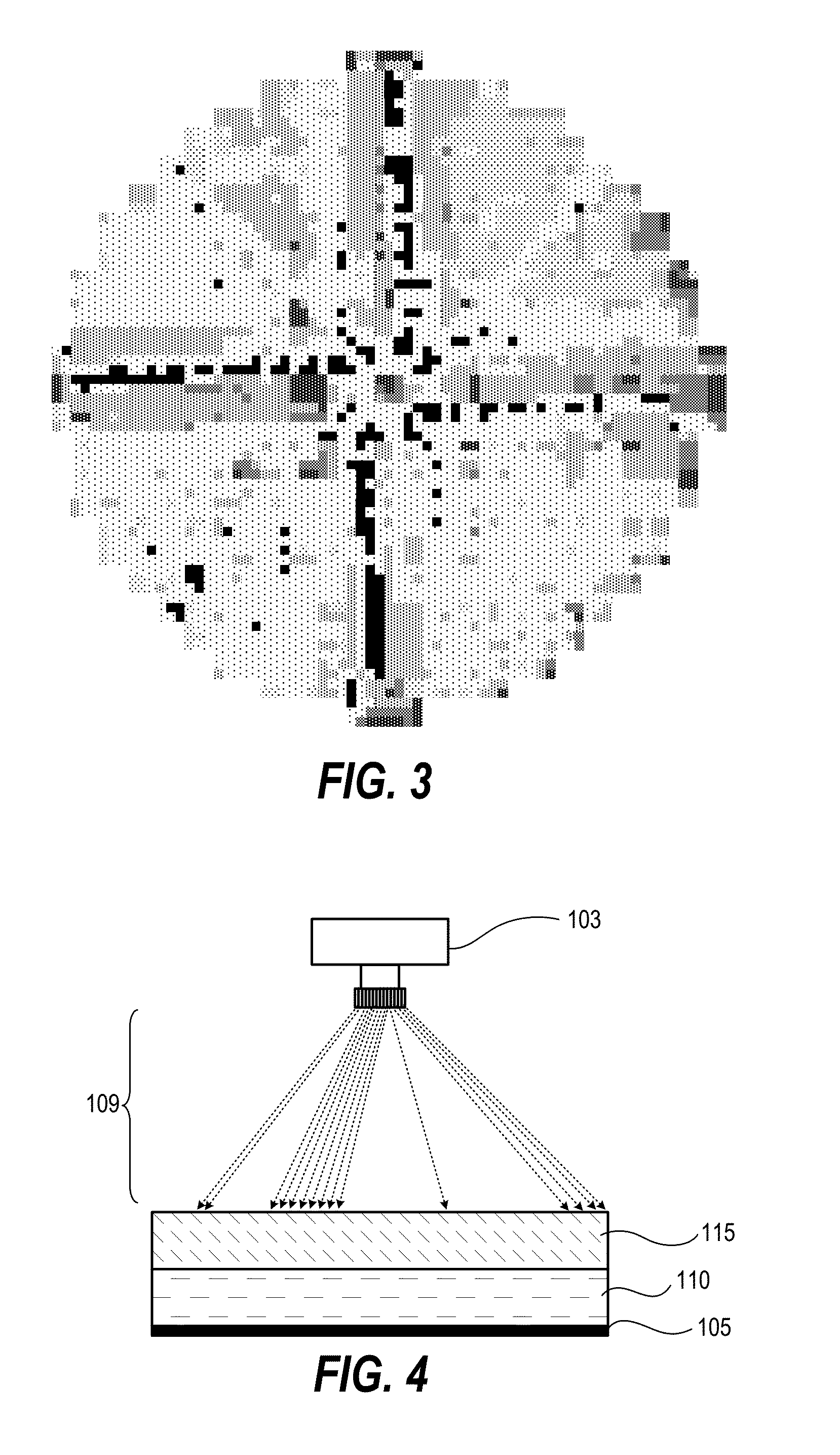
[0021]Techniques herein include systems and methods that provide a spatially-controlled or pixel-based projection of light onto a substrate to tune various substrate properties. Such pixel-based light projection can be used to tune various properties of substrates, including tuning of critical dimensions, heating uniformity, evaporative cooling, photolithographic flare, raster delay, and generation of photo-sensitive agents. Combining such pixel-based light projection with contact-based heating (for example, a hotplate) can achieve significant improvements in temperature uniformity across a surface of a substrate. Combining such pixel-based light projection with photolithographic patterning processes can improve processing uniformity and decrease defectivity.

[0022]In one embodiment, a digital light processing (DLP) chip, grating light valve (GLV), or other grid-based micro projection technology, coupled with a light source can focus an image (optionally using a lens) onto a substrat...


PUM


Abstract

Techniques herein include systems and methods that provide a spatially-controlled or pixel-based projection of light onto a substrate to tune various substrate properties. A given pixel-based image projected on to a substrate surface can be based on a substrate signature. The substrate signature can spatially represent non-uniformities across the surface of the substrate. Such non-uniformities can include energy, heat, critical dimensions, photolithographic exposure dosages, etc. Such pixel-based light projection can be used to tune various properties of substrates, including tuning of critical dimensions, heating uniformity, evaporative cooling, and generation of photo-sensitive agents. Combining such pixel-based light projection with photolithographic patterning processes and/or heating processes improves processing uniformity and decreases defectivity. Embodiments can include using a digital light processing (DLP) chip, grating light valve (GLV), or other grid-based micro projection technology.

Description

CROSS REFERENCE TO RELATED APPLICATIONS[0001]The present application claims the benefit of U.S. Provisional Patent Application No. 61 / 909,714, filed on Nov. 27, 2013, entitled “Optical Projection Tuned Hot Plate,” which is incorporated herein by reference in its entirety. The present application also claims the benefit of U.S. Provisional Patent Application No. 61 / 932,005, filed on Jan. 27, 2014, entitled “System and Method for Shifting Critical Dimensions of Patterned Films,” which is incorporated herein by reference in its entirety.BACKGROUND OF THE INVENTION[0002]This disclosure relates generally to patterning of substrates including semiconductor substrates such as silicon wafers. This disclosure also relates to processes involved with photolithography including coating and developing films on substrates as part of semiconductor device fabrication. This disclosure particularly relates to controlling dimensions and accuracy of patterned features as part of photolithography and pa...

Claims


Application Information

Patent Timeline
Patent Type & Authority Applications(United States)
IPC IPC(8): H01L21/66H01L21/027
CPCH01L21/027H01L22/20G03F7/168G03F7/40H01L21/67248H01L21/67253G03F7/70466G03F7/70558G03F7/70625G03F7/70991
Inventor DEVILLIERS, ANTON J.FULFORD, DANIELLEUSINK, GERRIT J.
Owner TOKYO ELECTRON LTD
Why Eureka
Try Eureka