

Scanning probe microscope and measuring method using same
a scanning probe and microscope technology, applied in scanning probe microscopy, measuring devices, instruments, etc., can solve the problems of high spatial resolution and difficulty in realizing scanning probe microscopes using physical quantities of weak signals, and achieve high spatial resolution and spatial resolution. high
- Summary
- Abstract
- Description
- Claims
- Application Information
AI Technical Summary
Benefits of technology
Problems solved by technology
Method used
Image

Examples
example 1
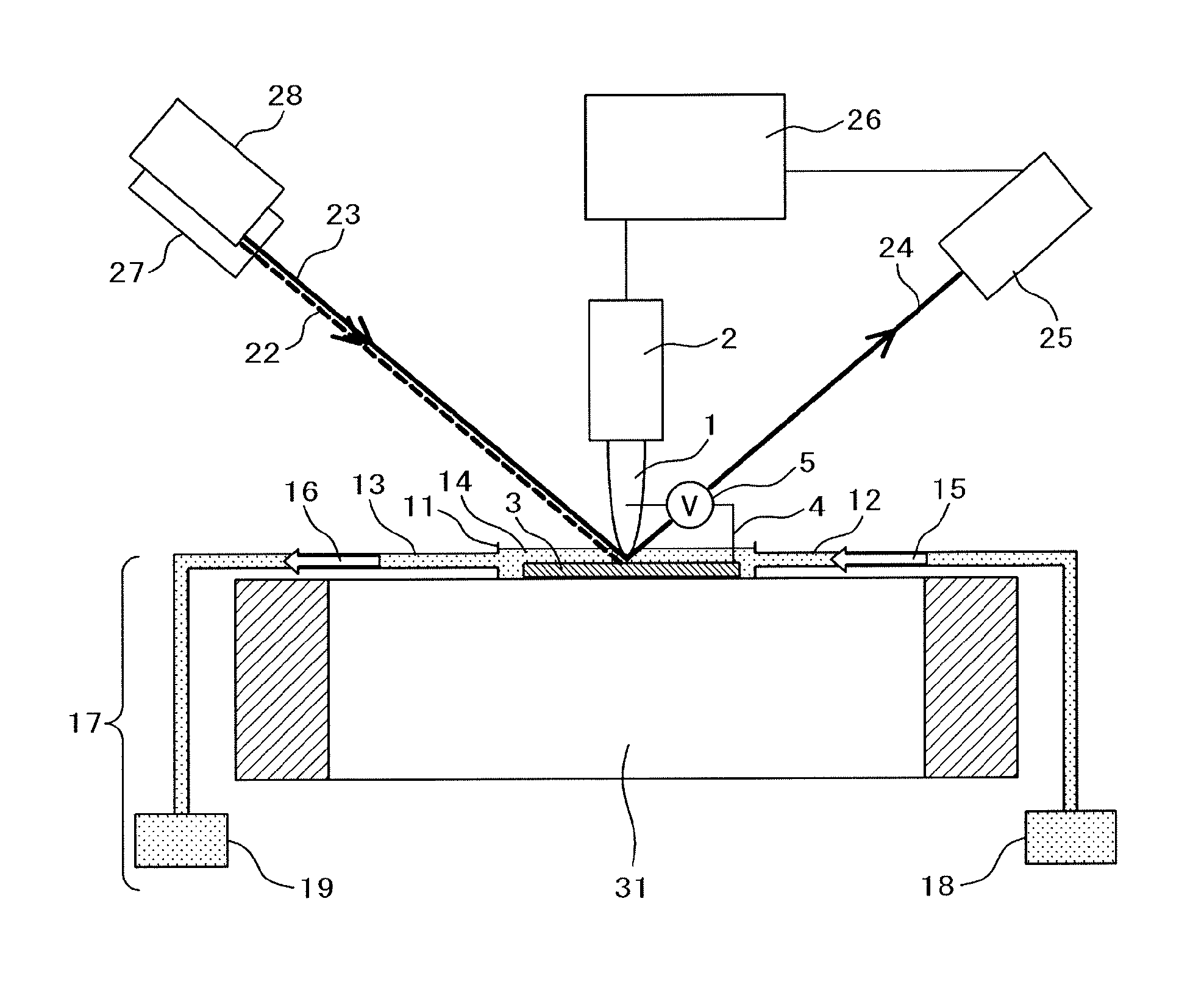
[0038]This section discloses a tip-enhanced scanning sum-frequency microscope as one form of a scanning probe microscope. FIG. 1 is a general structural diagram of a scanning probe microscope of a first embodiment of the present invention. A probing needle 1 is installed in an oscillator 2 and its position relative to a specimen 3 is controlled by the oscillator 2. As the material of the probing needle 1, a material is selected that, when the probing needle 1 has been positioned in incoming light, amplifies the intensity of near-field light and concentrates the light at or near the tip of the probing needle. If Raman scattering is used like Raman spectroscopy or sum-frequency generation spectroscopy among others, metals such as gold, silver, copper and aluminum and their compounds, which enable effective use of surface-enhanced Raman scattering, may be used. A probing needle with a gold thin film, 1 to 20 nm thick, evaporated on a silicon probing needle is used as an effective probi...
example 2
[0051]This section discloses a tip-enhanced scanning sum-frequency microscope by means of a total reflection method as one form of a scanning probe microscope. FIG. 6 is a general structural diagram of a scanning probe microscope of a second embodiment of the present invention.
[0052]Descriptions are provided, focusing on parts that differ from the scanning probe microscope of the first embodiment. In the present embodiment, a specimen 3 is installed on the upper surface of a prism 21. A specimen holder 11 has a ring-like shape or the thickness of its portion contacting with the prism 21 is very thin and a material that well transmits pulse oscillation laser lights is used. The specimen 3 is limited to a material that has a thin thickness and well transmits pulse oscillation laser lights. A pulse oscillation laser light which is input vertically, perpendicularly to the cylindrical surface of the prism 21 or plural pulse oscillation laser lights which are input synchronously are total...
example 3
[0053]This section discloses a tip-enhanced scanning second harmonic microscope as one form of a scanning probe microscope and other tip-enhanced scanning optical probe microscopes by means of linear and non-linear optical characteristics. In the present embodiment, descriptions are provided using FIG. 1, as is the case for the first embodiment.
[0054]In a tip-enhanced scanning second harmonic microscope according to the present embodiment, a first pulse oscillation laser light 22 which is an infrared pulse oscillation laser light with a wavelength of 1064 nm is input at or near a spot on a specimen 3 where the probing needle 1 gets close to. Output light 24 is input to the filter-equipped detector 25 and the light intensity at a frequency that is twice as much as the frequency of the first pulse oscillation laser light 22 is measured. Cultured nerve cells are used as the specimen 3. While measuring irregularities of the nerve cells by AFM, by mapping the second harmonic intensity, i...
PUM
 Abstract
Description
Claims
Application Information