Organic light emitting diode display device and method of fabricating the same

a light-emitting diode and display device technology, applied in the direction of solid-state devices, transistors, thermoelectric devices, etc., can solve the problem of difficult to obtain sufficient capacitance of storage capacitors cst, and achieve the effect of increasing the capacitance of storage capacitors, improving aperture ratio and brightness, and increasing design margins

Active Publication Date: 2015-06-25
LG DISPLAY CO LTD
View PDF14 Cites 52 Cited by
  • Summary
  • Abstract
  • Description
  • Claims
  • Application Information

AI Technical Summary

Benefits of technology

[0017]An object of the present disclosure is to provide an organic light emitting diode display device and a method of fabricating the same that increase capacitance of a storage capacitor and improve the aperture ratio and brightness.
[0018]Another object of the present disclosure is to provide organic light emitting diode display device and a method of fabricating the same that increase design margins.

Problems solved by technology

Accordingly, it is difficult to obtain sufficient capacitance of the storage capacitor Cst.

Method used


Image

  • Organic light emitting diode display device and method of fabricating the same
  • Organic light emitting diode display device and method of fabricating the same
  • Organic light emitting diode display device and method of fabricating the same

Examples


Embodiment Construction

[0031]Reference will now be made in detail to the preferred embodiment, examples of which are illustrated in the accompanying drawings.

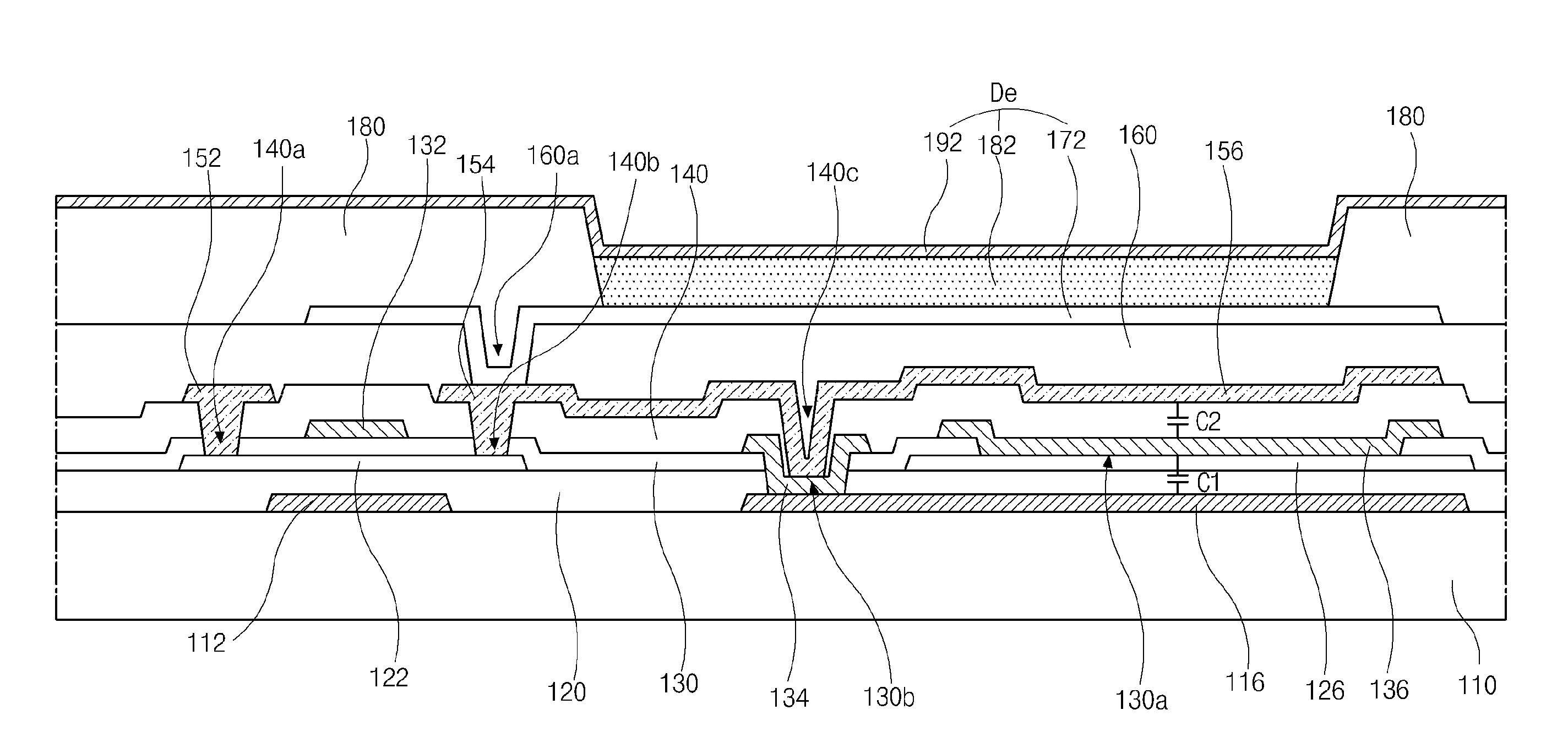
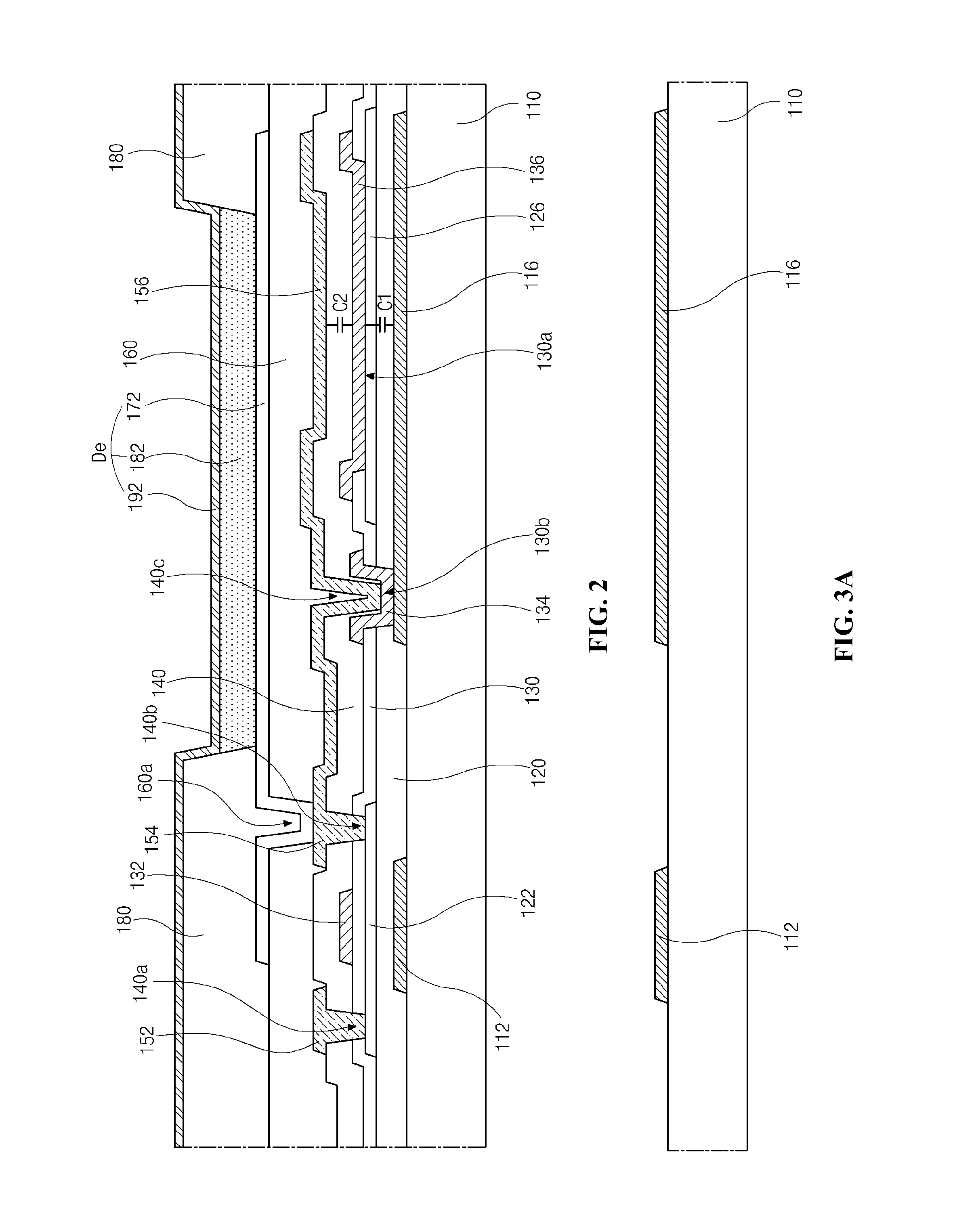
[0032]FIG. 2 is a cross-sectional view of an OLED display device according to an embodiment of the present invention. FIG. 2 shows one pixel region.

[0033]In FIG. 2, a light-blocking layer 112 and a first capacitor electrode 116 of a conductive material such as metal are formed on an insulating substrate 110.

[0034]A buffer layer 120 of an insulating material is formed on the light-blocking layer 112 and the first capacitor electrode 116 substantially all over the substrate 110.

[0035]A first oxide semiconductor layer 122 and a second oxide semiconductor layer 126 of an oxide semiconductor material are formed on the buffer layer 120. The first oxide semiconductor layer 122 is disposed over the light-blocking layer 112, and the second oxide semiconductor layer 126 is disposed over the first capacitor electrode 116. The first oxide semiconductor layer 122...


PUM


Abstract

An organic light emitting diode display device comprises a driving thin film transistor including a first semiconductor layer, a gate insulating layer formed on the first semiconductor layer. The device further includes a storage capacitor including a first capacitor electrode electrically coupled to a drain electrode of the driving thin film transistor, a buffer layer formed on the first capacitor electrode, a second semiconductor layer formed on the buffer layer, and a second capacitor electrode formed on the second semiconductor layer and electrically coupled to a gate electrode of the driving thin film transistor. The device also includes an organic light emitting diode connected to the drain electrode of the driving transistor. The gate insulating layer has at least one hole in a region where the gate insulating layer overlaps the second semiconductor layer, thereby exposing the second semiconductor layer to the second capacitor electrode.

Description

CROSS-REFERENCE TO RELATED APPLICATION[0001]The present application claims the priority benefit of Korean Patent Application No. 10-2013-0161519 filed in the Republic of Korea on Dec. 23, 2013, which is hereby incorporated by reference in their entirety.BACKGROUND[0002]1. Field of the Disclosure[0003]The present disclosure relates to an organic light emitting diode display device, and more particularly, to an organic light emitting diode display device that increases capacitance of a storage capacitor and a method of fabricating the same.[0004]2. Discussion of the Related Art[0005]Recently, flat panel displays have been widely developed and applied to various fields because of their thin profile, light weight, and low power consumption.[0006]Among the flat panel displays, organic light emitting diode (OLED) display devices, which may be referred to as organic electroluminescent display devices, emit light during loss of electron-hole pairs formed by injecting charges into a light em...

Claims


Application Information

Patent Timeline
Patent Type & Authority Applications(United States)
IPC IPC(8): H01L27/32H01L27/12H01L51/56H01L29/786
CPCH01L27/3272H01L27/3262H01L27/3265H01L2227/323H01L29/7869H01L27/1259H01L51/56H01L27/3258H01L27/1225H01L27/1255H01L27/124H10K59/1216H10K59/1201H10K59/00H01L21/82H01L21/28008H01L2021/775H10K59/10H10K59/12H10K59/126
Inventor LEE, YOUNG-JANGJEONG, HO-YOUNG
Owner LG DISPLAY CO LTD
Why Eureka
Try Eureka