Method device and operation method of said device

a technology of tunnel field effect transistor and method device, which is applied in the direction of semiconductor devices, digital storage, instruments, etc., can solve the problems of deteriorating reliability and the life of the devi

Active Publication Date: 2015-06-25
ECOLE POLYTECHNIQUE FEDERALE DE LAUSANNE (EPFL)
View PDF3 Cites 27 Cited by
  • Summary
  • Abstract
  • Description
  • Claims
  • Application Information

AI Technical Summary

Problems solved by technology

In conventional metal-oxide-semiconductor (MOS) FET structure (p+ / i / +p or n+ / i+ / n), the desired potential well is inherently available and it is exploited with floating body effect in Z-RAM [0]; however the majority carrier injection to the body requires techniques (i.e. hot carrier injection) which degrade reliability and the device's life time.

Method used


Image

  • Method device and operation method of said device
  • Method device and operation method of said device
  • Method device and operation method of said device

Examples


Embodiment Construction

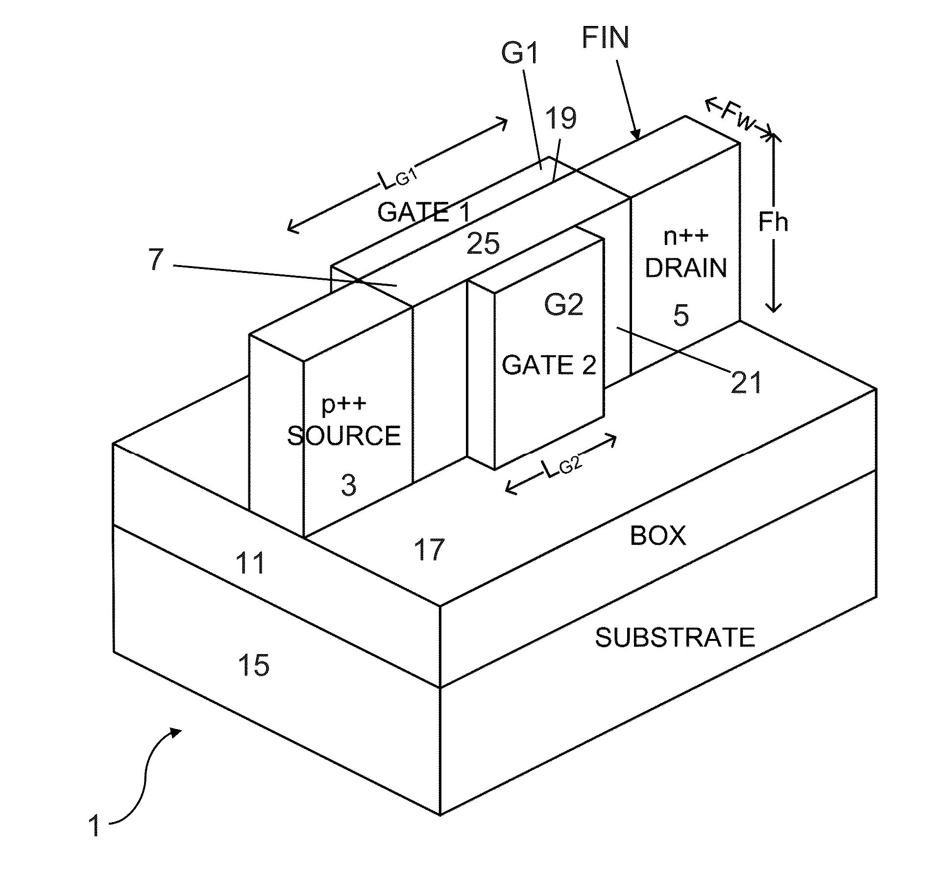
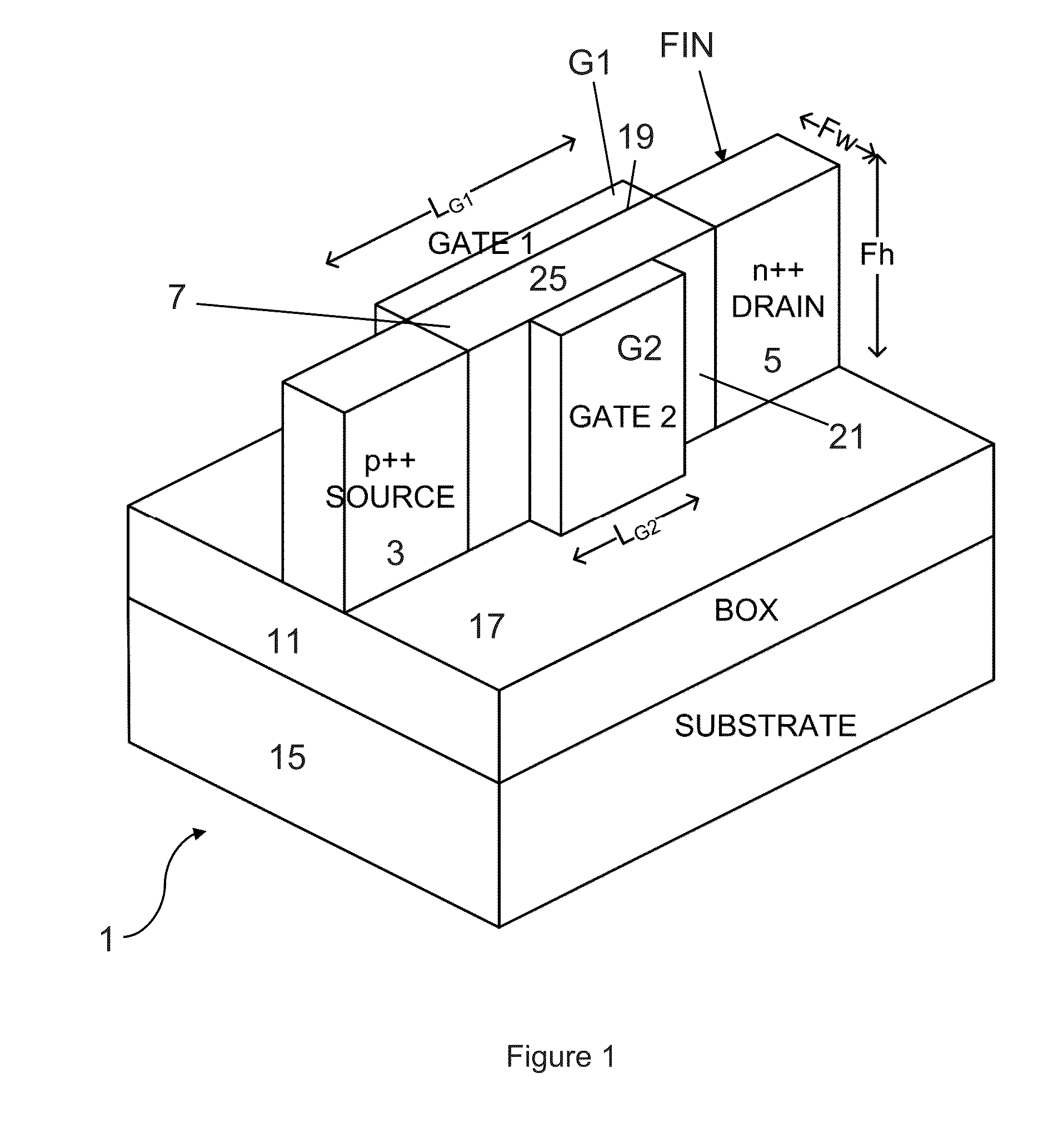
[0043]FIG. 1 illustrates a device 1 according to a first embodiment of the present invention. The device 1 is a three dimensional Double Gate FIN N-type Tunnelling Field Effect Transistor (3D DG FIN NTFET) structure with a partial side gate. The device includes a non-planar, double-gate transistor built on an SOI or silicon substrate, that is, a FIN double-gate transistor built on an SOI or silicon substrate.

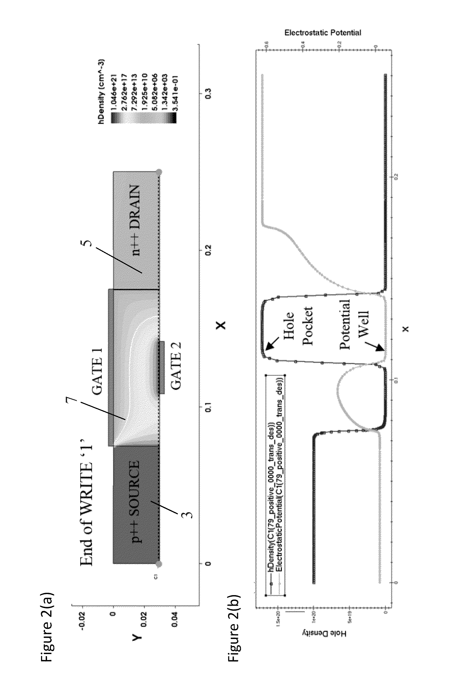
[0044]The device 1 includes a fin structure (FIN) and the device 1 is a non-planer structure. The fin structure comprises a source region 3, a drain region 5, an intrinsic channel region 7 between the drain region 5 and the source region 3 and connected to said source and drain regions, a first gate Gate1 (G1) connected to the intrinsic channel region 7 for transistor control, and a second gate Gate2 (G2) connected to the intrinsic channel region 7 to generate a potential well for storing mobile charge carriers to permit memory operation.

[0045]The device 1 further includes a BOX...


PUM


Abstract

The present invention relates to a single field effect transistor capacitor-less memory device including a drain region, a source region, an intrinsic channel region between the drain region and the source region forming the single field effect transistor and a base.The device further includes a fin structure comprising the source region, the intrinsic channel and the drain region, the fin structure extending outwardly from the base, and a double gate comprising a first gate connected to a first exposed lateral face of the intrinsic channel region for transistor control, and a second gate connected to a second exposed lateral face of the intrinsic channel region to generate a potential well for storing mobile charge carriers permitting memory operation, the first gate and the second gate being asymmetric for asymmetric electrostatic control of the device.The present invention also relates to a method for operating said device.

Description

CROSS-REFERENCE TO RELATED APPLICATIONS[0001]This application claims the benefit of International Application No. PCT / IB2013 / 060708 filed Dec. 6, 2013, the entire contents of which are incorporated herein by reference.[0002]The present invention concerns the field of transistors, in particular the subset which is dedicated to volatile memory design and, more particularly, a single transistor capacitor-less dynamic random access memory device. The invention further relates to methods of operation of the device, a memory cell including the device and an array comprising a plurality of said memory cells. The invention further concerns a method of operating said memory cell array.[0003]In particular, a capacitor-less dynamic random access memory (DRAM) device comprising a double gate p / i / n structure is described as well as methods of operation of said device.[0004]The device and gain cells feature memory like operation thanks to the creation of an energy pocket in a channel region by a ...

Claims


Application Information

Patent Timeline
Patent Type & Authority Applications(United States)
IPC IPC(8): H01L29/78H01L27/108G11C11/409H01L27/12
CPCH01L29/7855G11C11/409H01L27/10802H01L27/1211G11C11/404G11C2211/4016H01L29/7391H10B12/20H10B12/056
Inventor BISWAS, ARNABDAGTEKIN, NILAYIONESCU, MIHAI ADRIAN
Owner ECOLE POLYTECHNIQUE FEDERALE DE LAUSANNE (EPFL)
Why Eureka
Try Eureka