Substrate processing system, method of manufacturing semiconductor device and non-transitory computer-readable recording medium

a processing system and semiconductor technology, applied in the direction of mechanical equipment, water supply installation, transportation and packaging, etc., can solve the problems of reducing processing temperature, reducing manufacturing throughput, and becoming difficult to perform miniaturization, so as to improve manufacturing throughput and improve the characteristics of the film formed on the substrate.

Inactive Publication Date: 2015-07-02
KOKUSA ELECTRIC CO LTD
View PDF26 Cites 203 Cited by
  • Summary
  • Abstract
  • Description
  • Claims
  • Application Information

AI Technical Summary

Benefits of technology

[0009]The present invention is directed to provide a substrate processing system, a method of manufacturing a semiconductor device and a non-transitory computer-readable recording medium that are capable of improving characteristics of a film formed on a substrate and improving manufacturing throughput.

Problems solved by technology

Since a minimum machining dimension of the semiconductor device represented by an LSI, a dynamic random access memory (DRAM), or a flash memory in recent times is smaller than 30 nm, it is becoming difficult to perform miniaturization, improve manufacturing throughput and reduce a processing temperature, all while maintaining quality.
In the film forming method, for example, when the plasma is generated, since power regulation, pressure regulation, gas concentration regulation, and so on, are time-consuming, reduction in manufacturing throughput is limited.

Method used


Image

  • Substrate processing system, method of manufacturing semiconductor device and non-transitory computer-readable recording medium
  • Substrate processing system, method of manufacturing semiconductor device and non-transitory computer-readable recording medium
  • Substrate processing system, method of manufacturing semiconductor device and non-transitory computer-readable recording medium

Examples


Embodiment Construction

[0028]Hereinafter, embodiments of the present invention will be described.

Embodiments of the Present Invention

[0029]Hereinafter, an embodiment of the present invention will be described with reference to the accompanying drawings.

[0030](1) Configuration of Substrate Processing Apparatus

[0031]First, a substrate processing apparatus according to an embodiment of the present invention will be described.

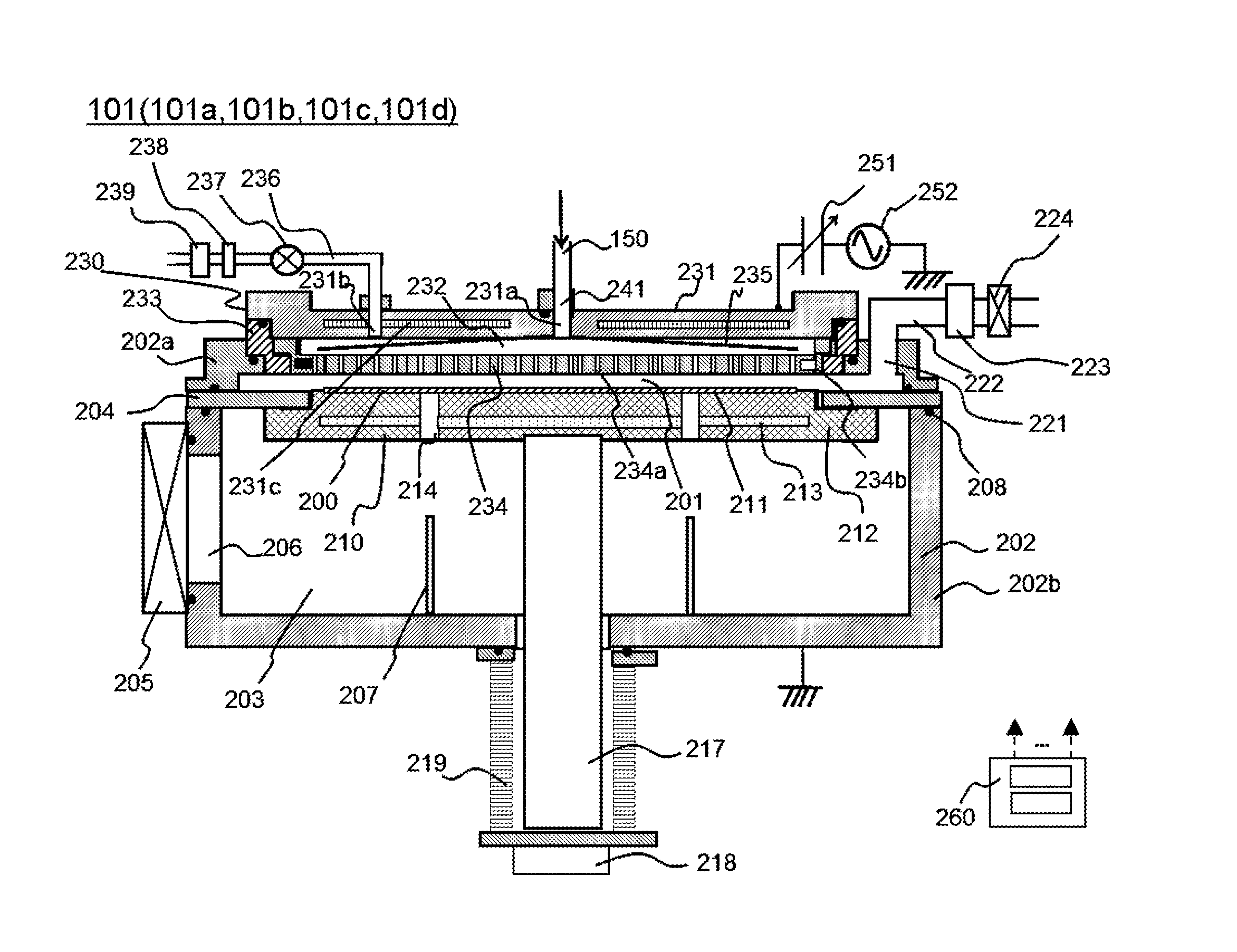
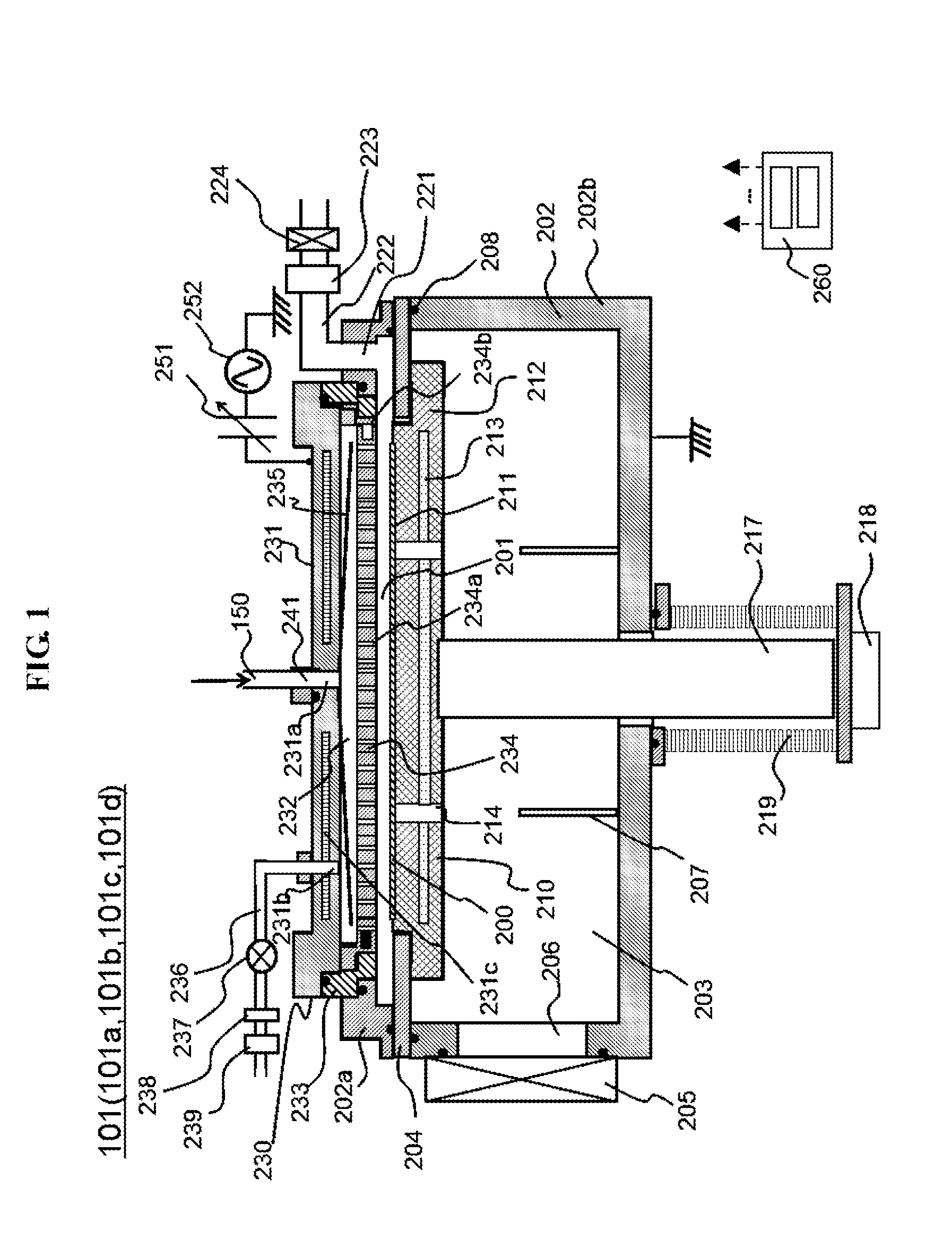
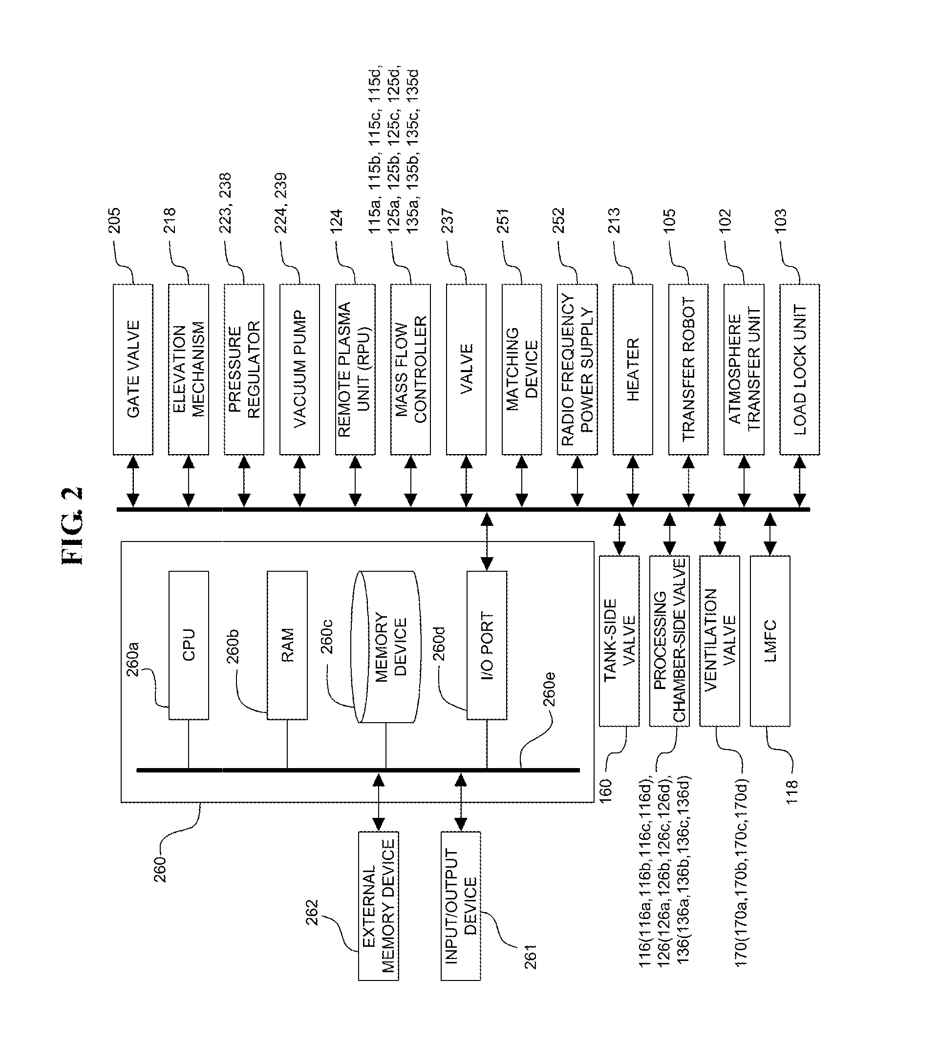
[0032]A substrate processing apparatus 101 according to the embodiment will be described. The substrate processing apparatus 101 is a high-k insulating film forming unit, and as shown in FIG. 1, is configured as a single-type substrate processing apparatus. In the substrate processing apparatus, as described above, a process of manufacturing a semiconductor device is performed.

[0033]As shown in FIG. 1, the substrate processing apparatus 101 includes a processing container 202. The processing container 202 is constituted by a sealed container having a circular and flat transverse section....


PUM

PropertyMeasurementUnit
pressureaaaaaaaaaa
temperatureaaaaaaaaaa

Abstract

A substrate processing system includes a plurality of processing chambers accommodating substrates, a processing gas supply system configured to supply a processing gas sequentially into the plurality of processing chambers, a reactive gas supply system configured to supply an activated reactive gas sequentially into the plurality of processing chambers, a buffer tank installed at the processing gas supply system, and a control unit configured to control the processing gas supply system and the reactive gas supply system such that a time period of supplying the reactive gas into one of the plurality of processing chambers is equal to a sum of a time period of supplying the processing gas into the one of the plurality of processing chambers and a time period of supplying the processing gas into the buffer tank, and the processing gas and the reactive gas are alternately supplied into the plurality of processing chambers.

Description

CROSS-REFERENCE TO RELATED PATENT APPLICATION[0001]This U.S. non-provisional patent application claims priority under 35 U.S.C. §119 of Japanese Patent Application Nos. 2013-271924 and 2014-040430 filed on Dec. 27, 2013 and Mar. 3, 2014, respectively, in the Japanese Patent Office, the entire contents of which are hereby incorporated by reference.BACKGROUND OF THE INVENTION[0002]1. Field of the Invention[0003]The present invention relates to a substrate processing system, a method of manufacturing a semiconductor device and a non-transitory computer-readable recording medium.[0004]2. Description of the Related Art[0005]Circuit patterns are being finely miniaturized as large scale integrated circuits (hereinafter referred to as LSIs) become more highly integrated.[0006]In order to integrate a large number of semiconductor devices in a small area, a size of the device should be reduced, and for this, a width and a gap of patterns to be formed should be reduced.[0007]In burying a fine ...

Claims


Application Information

Patent Timeline
Patent Type & Authority Applications(United States)
IPC IPC(8): H01L21/67
CPCH01L21/67017C23C16/34C23C16/405C23C16/4408C23C16/452C23C16/45523C23C16/45561C23C16/52Y10T137/0318H01L21/02274
Inventor SATO, TAKETOSHI
Owner KOKUSA ELECTRIC CO LTD
Why Eureka
Try Eureka