Stacked Bi-layer as the low power switchable RRAM

a low-power switchable, stacked bi-layer technology, applied in the direction of bulk negative resistance effect devices, basic electric elements, electrical apparatus, etc., can solve the problems of over-programming, over-current through the resistive switching layer, and over-programming, and achieve constant resistance

Active Publication Date: 2015-07-02
INTERMOLECULAR
View PDF4 Cites 12 Cited by
  • Summary
  • Abstract
  • Description
  • Claims
  • Application Information

AI Technical Summary

Benefits of technology

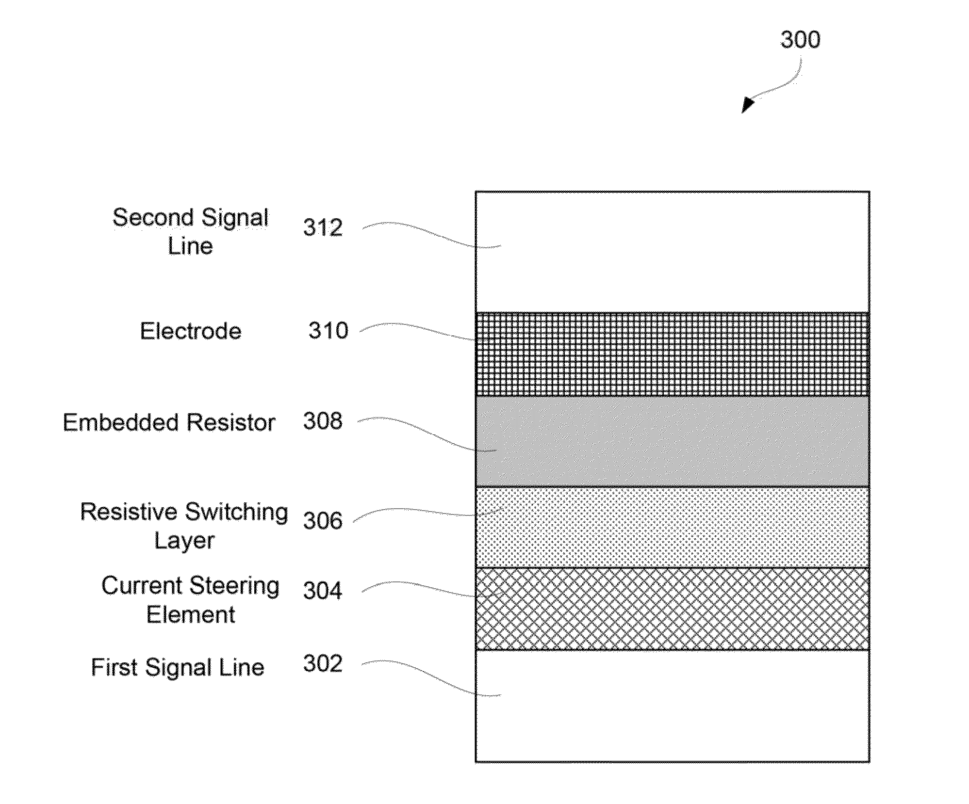
[0004]Provided are resistive random access memory (ReRAM) cells and methods of fabricating thereof. Resistive switching nonvolatile memory elements may include a first layer formed on a substrate. The first layer may be operable as a bottom electrode. The resistive switching nonvolatile memory elements may further include a second layer formed over the first layer. The second layer may be operable as a resistive switching layer that is configured to switch between at least a first resistive state and a second resistive state. The resistive switching nonvolatile memory elements may also include a third layer formed over the second layer. The third layer may be operable as a resistive layer having a substantially constant resistance. The third layer may be configured to determine, at least in part, an electrical resistivity of the resistive switching nonvolatile memory element. The third layer may include a semi-metallic material. The semi-metallic material may be, at least in part, amorphous. Moreover, the resistive switching nonvolatile memory elements may include a fourth layer formed over the third layer. The fourth layer may be operable as a top electrode.

Problems solved by technology

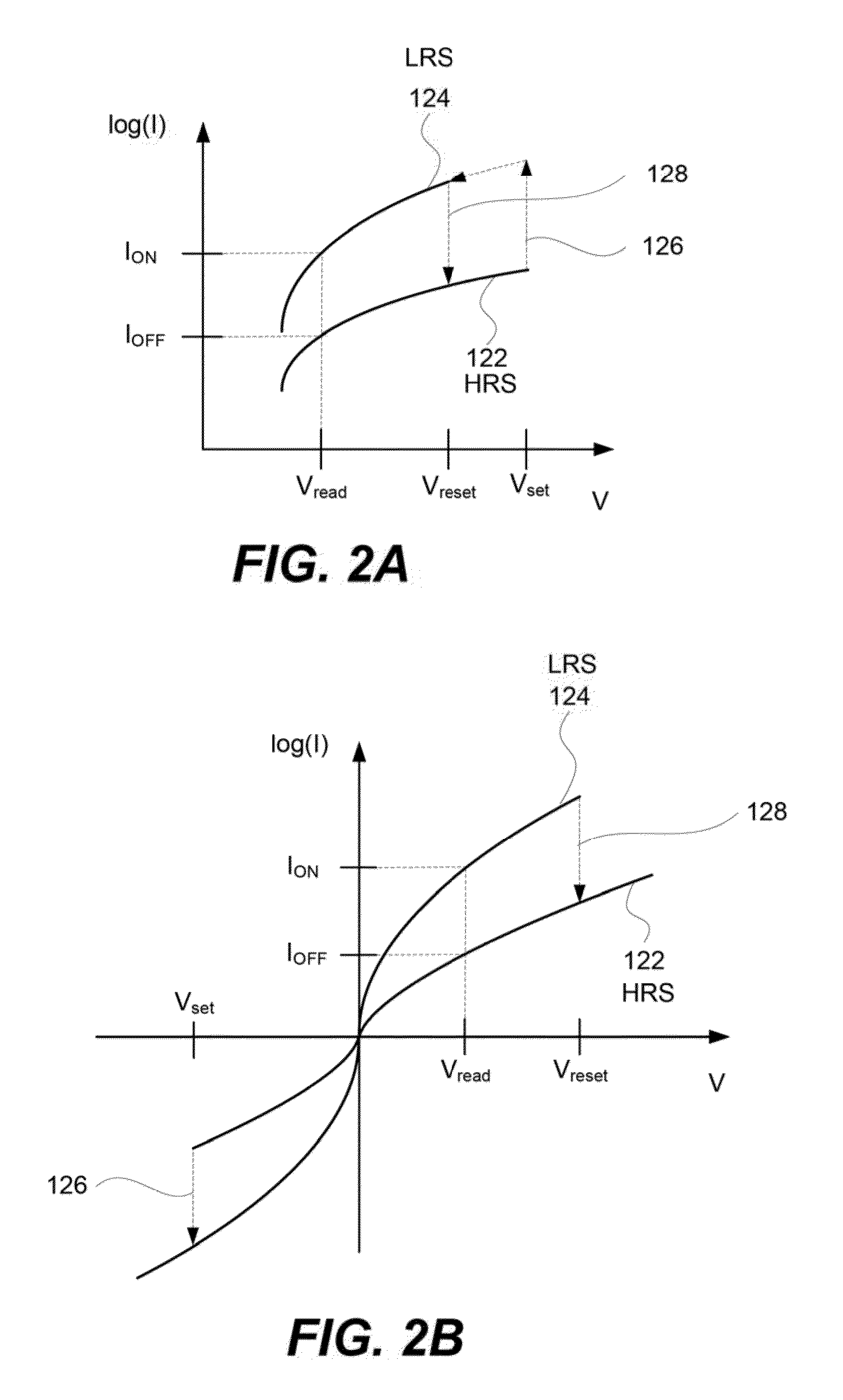
For example, when the resistive switching layer is switched from its high resistive state (HRS) to its low resistive state (LRS), a rapid drop in resistance associated with this switch may cause an excessive current through the resistive switching layer and an over-programming.
However, shorter pulses have their own inherent limitations, such as requiring more pulses or higher voltages to achieve the same switching result, which may consume more power than fewer, longer, lower-voltage pulses.
Furthermore, even during a relatively short switching pulse, the change in resistance may be sufficiently large to result in current spiking and over-programming.
Conventional embedded resistors often do not provide a full combination of good resistivity, good diffusion barrier characteristics, and a good reservoir of oxygen vacancies.
However, these materials might not provide a sufficient reservoir of oxygen vacancies for prolonged switching of the memory element and might also not provide a sufficient migration barrier to prevent migration of materials included in other layers, such as titanium which may be included in an electrode of the memory element.
Moreover, other conventional embedded resistors may provide sufficient reservoirs of oxygen vacancies, but might have resistances that are too high to allow low voltage operation of the memory element.
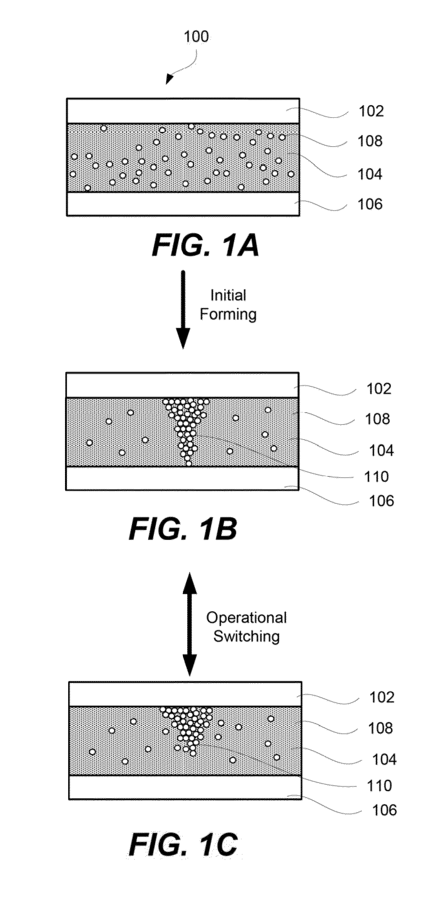
That is, defects may travel through an interface formed by this electrode with the resistive switching layer (i.e., the reactive interface).
Furthermore, there may be some mobility of defects within resistive switching layer 104.
This breakage generally does not correspond to complete dispersion of defects forming these conductive paths and may be a self-limiting process, i.e., the process may stop after some initial breakage occurs.
As previously discussed, conventional embedded resistors are limited because they are not able to provide all of these properties simultaneously.

Method used


Image

  • Stacked Bi-layer as the low power switchable RRAM
  • Stacked Bi-layer as the low power switchable RRAM
  • Stacked Bi-layer as the low power switchable RRAM

Examples


Embodiment Construction

[0020]A detailed description of various embodiments is provided below along with accompanying figures. The detailed description is provided in connection with such embodiments, but is not limited to any particular example. The scope is limited only by the claims and numerous alternatives, modifications, and equivalents are encompassed. Numerous specific details are set forth in the following description in order to provide a thorough understanding. These details are provided for the purpose of example and the described techniques may be practiced according to the claims without some or all of these specific details. For the purpose of clarity, technical material that is known in the technical fields related to the embodiments has not been described in detail to avoid unnecessarily obscuring the description.

INTRODUCTION

[0021]A ReRAM cell exhibiting resistive switching characteristics generally includes multiple layers formed into a stack, such as a “metal-insulator-metal” (MIM) stack...


PUM


Abstract

Provided are resistive random access memory (ReRAM) cells and methods of fabricating thereof. The resistive switching nonvolatile memory cells may include a first layer disposed. The first layer may be operable as a bottom electrode. The resistive switching nonvolatile memory cells may also include a second layer disposed over the first layer. The second layer may be operable as a resistive switching layer that is configured to switch between a first resistive state and a second resistive state. The resistive switching nonvolatile memory cells may include a third layer disposed over the second layer. The third layer may be operable as a resistive layer that is configured to determine, at least in part, an electrical resistivity of the resistive switching nonvolatile memory element. The third layer may include a semi-metallic material. The resistive switching nonvolatile memory cells may include a fourth layer that may be operable as a top electrode.

Description

BACKGROUND[0001]Nonvolatile memory is computer memory capable of retaining stored information even when unpowered. Non-volatile memory is typically used for secondary storage or long-term persistent storage and may be used in addition to volatile memory, which loses the stored information when unpowered. Nonvolatile memory can be permanently integrated into computer systems (e.g., solid state hard drives) or can take the form of removable and easily transportable memory cards (e.g., USB flash drives). Nonvolatile memory is becoming more popular because of its small size / high density, low power consumption, fast read and write rates, retention, and other characteristics.[0002]Flash memory is a common type of nonvolatile memory because of its high density and low fabrication costs. Flash memory is a transistor-based memory device that uses multiple gates per transistor and quantum tunneling for storing the information on its memory device. Flash memory uses a block-access architecture...

Claims


Application Information

Patent Timeline
Patent Type & Authority Applications(United States)
IPC IPC(8): H01L45/00
CPCH01L45/1266H01L45/146H01L45/1633H01L45/08H01L45/1625H10B63/20H10B63/80H10B63/84H10N70/24H10N70/801H10N70/826H10N70/883H10N70/011H10N70/8416H10N70/026H10N70/028H10N70/828H10N70/841H10N70/8833
Inventor WANG, YUNNARDI, FEDERICOWELING, MILIND
Owner INTERMOLECULAR
Why Eureka
Try Eureka