

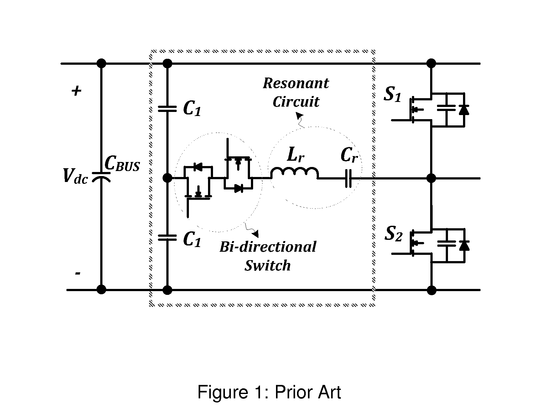
Zvs voltage source inverter
a voltage source inverter and zero voltage technology, applied in the field of electronic circuits, can solve the problems of low switching frequency, unavoidable reverse recovery losses of body diodes of power semiconductors, and overall losses of power conditioning systems, so as to eliminate the reverse recovery losses, eliminate the switching losses of power semiconductors, and improve the effect of quality
- Summary
- Abstract
- Description
- Claims
- Application Information
AI Technical Summary
Benefits of technology
Problems solved by technology
Method used
Image

Examples
Embodiment Construction
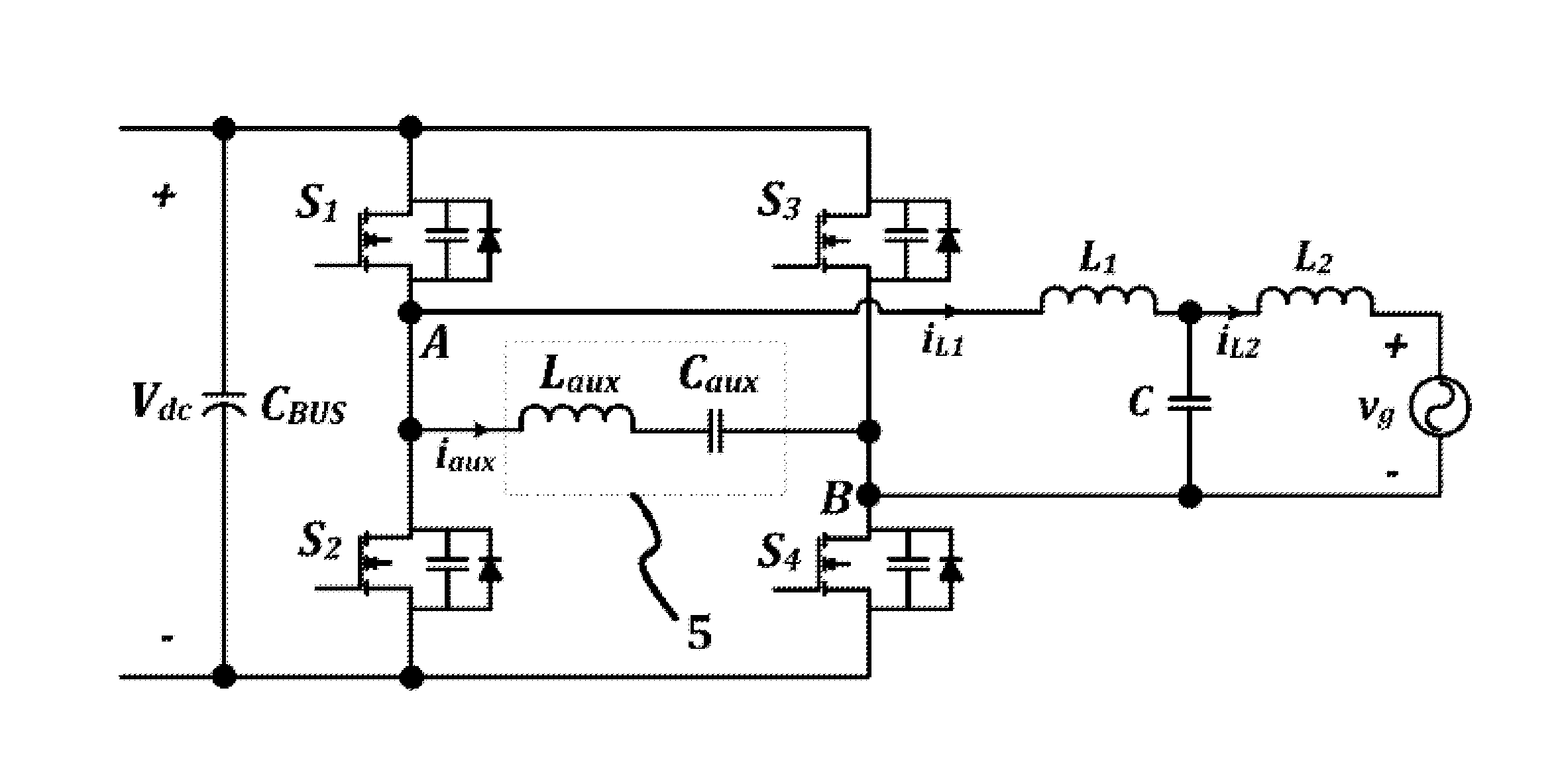
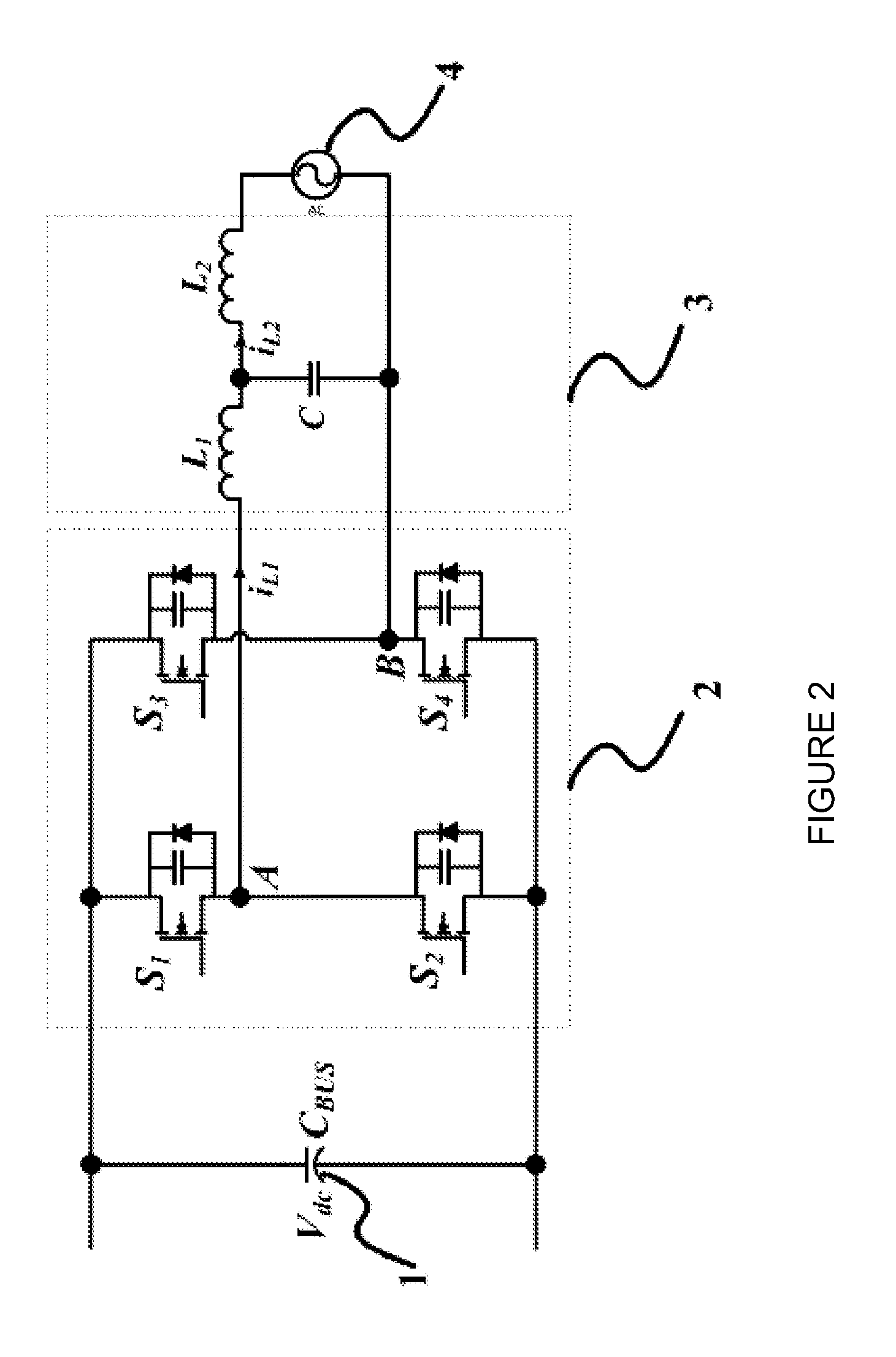
[0048]In one aspect, the present invention provides soft-switching circuits along with control methods for a single-phase voltage source inverter.
[0049]Switching losses are one of the main sources of power losses in a single-phase voltage source inverter. Switching losses are due to the overlap between the voltage across the power semiconductor and the current flowing through the power semiconductor during switching transitions. The switching losses are proportionally related to the switching frequency of the inverter. Therefore, in order to have a reasonable amount of losses the switching frequency of the inverter is limited, depending on the application (the switching frequency is usually between 10-20 kHz. Voltage source inverters operating with low switching frequency require a large filter in order to attenuate the switching noise and produce a high quality output current. In addition, a high amount of current ripple caused by a low switching frequency across the filter inducto...
PUM
 Abstract
Description
Claims
Application Information