Photodetector

Inactive Publication Date: 2015-07-30
ELECTRONICS & TELECOMM RES INST
View PDF2 Cites 10 Cited by
  • Summary
  • Abstract
  • Description
  • Claims
  • Application Information

AI Technical Summary

Benefits of technology

[0013]The following description relates to a photodetector capable of improving dark currents and responsi

Problems solved by technology

Since the wavelength range of light that silicon is able to absorb is between 400 nm and 700 nm, silicon is not applicable to general optical communications within a long w

Method used


Image

  • Photodetector
  • Photodetector
  • Photodetector

Examples


Embodiment Construction

[0024]The following description is provided to assist the reader in gaining a comprehensive understanding of the methods, apparatuses, and / or systems described herein. Accordingly, various changes, modifications, and equivalents of the methods, apparatuses, and / or systems described herein will be suggested to those of ordinary skill in the art. Also, descriptions of well-known functions and constructions may be omitted for increased clarity and conciseness.

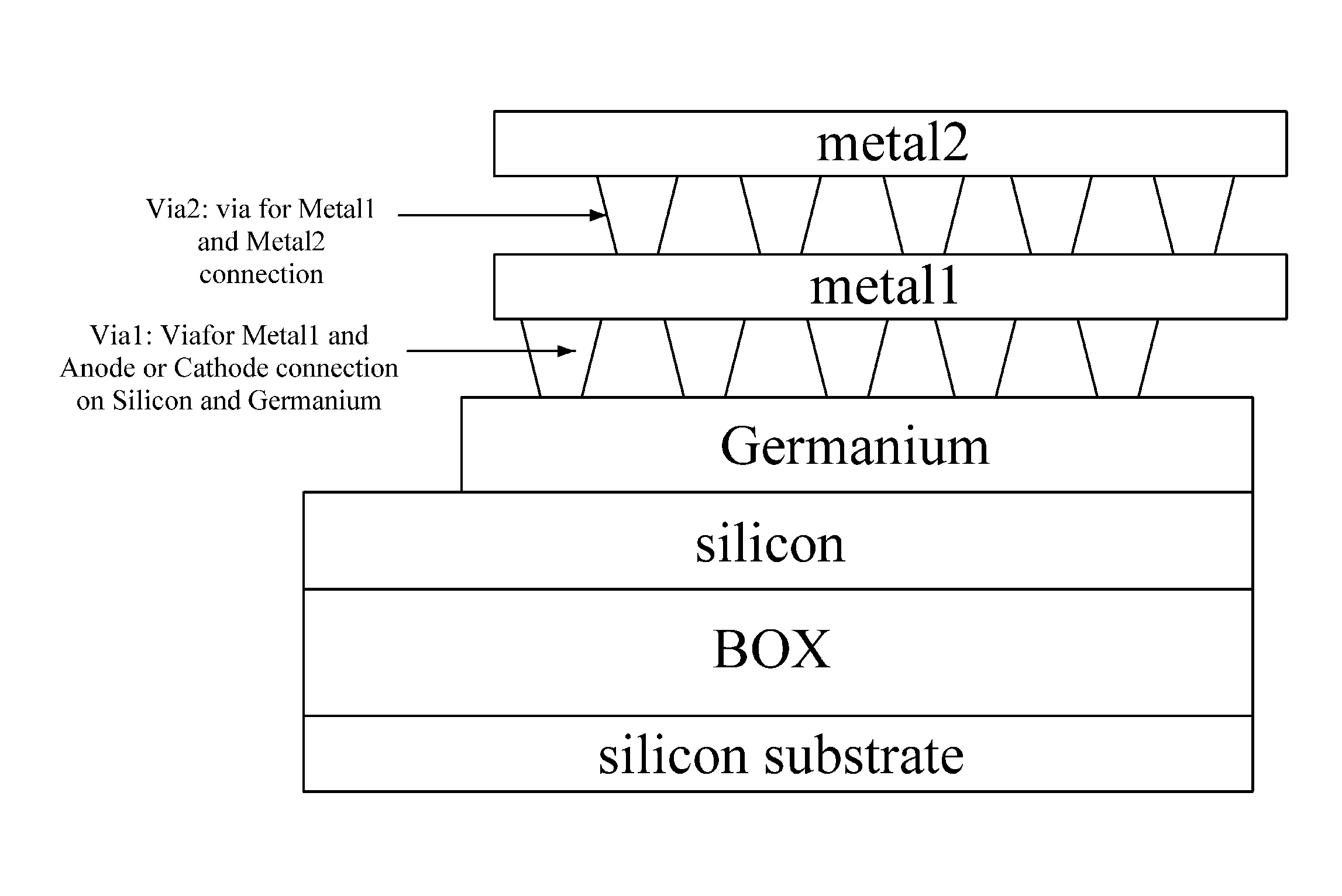
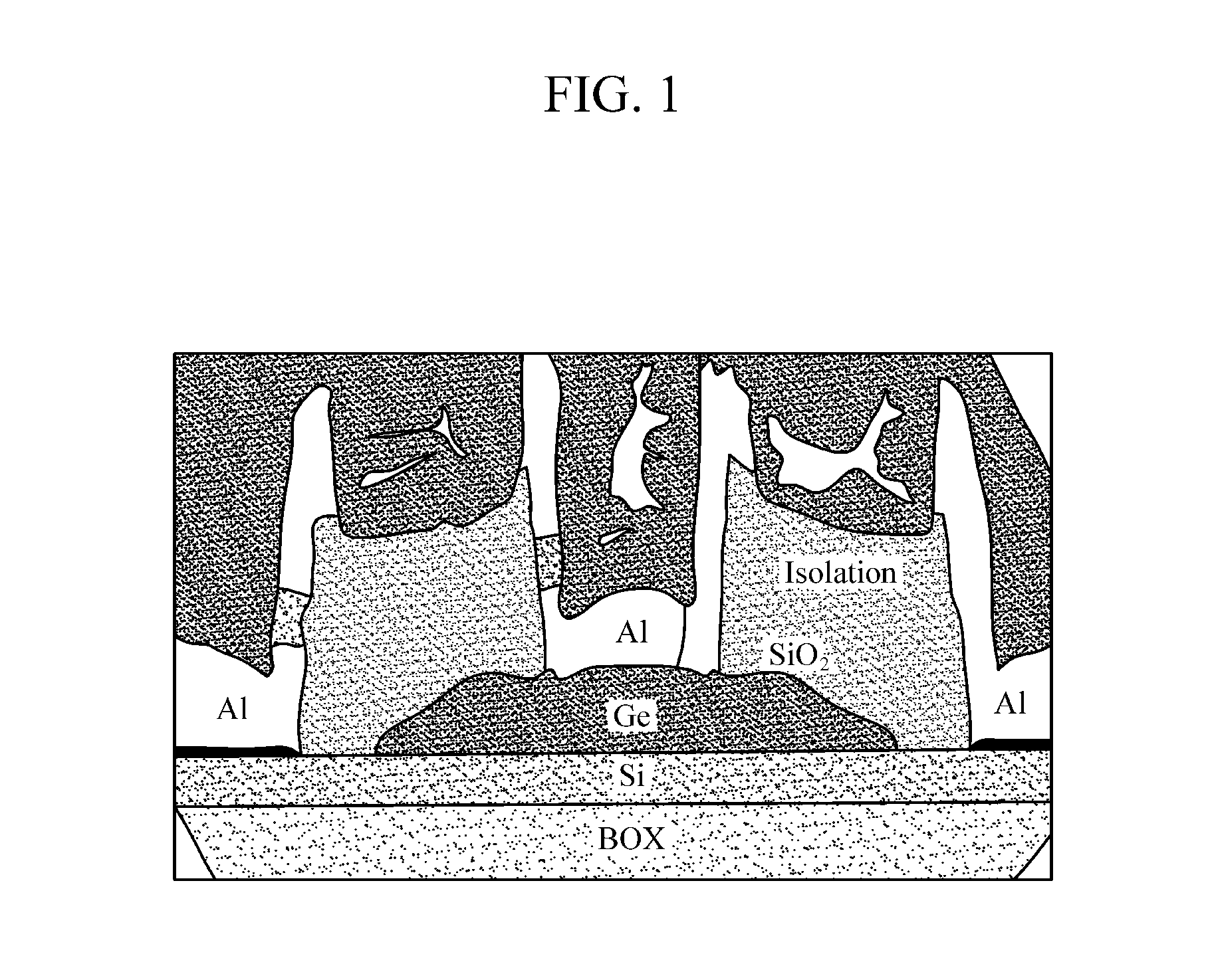
[0025]FIG. 1 is a diagram illustrating an example of an evanescent-coupled photodetector.

[0026]Referring to FIG. 1, a structure of a photodetector, developed by the Institute of Microelectronics in Singapore, is illustrated to show that a metal (Aluminum) is formed as a single via with a length corresponding to a length of the photodetector when connected to parts doped with different types within silicon and germanium regions. In this case, while a via resistance is reduced, a leakage current is disadvantageously increased due to...


PUM


Abstract

A photodetector is provided. The photodetector includes first metal layers in which optical signals are converted into electric signals; first vias formed between the first metal layers and doped areas which include doped areas on both ends of an optical waveguide and a doped area on a growing portion, which absorbs a light signal transmitted through the optical waveguide; second metal layer in which optical signals are converted into electric signals; and second vias formed between the first metal layers and the second metal layers.

Description

CROSS-REFERENCE TO RELATED APPLICATION(S)[0001]This application claims priority under 35 U.S.C. §119(a) from Korean Patent Application No. 10-2014-0009157, filed on Jan. 24, 2014, in the Korean Intellectual Property Office, the entire disclosure of which is incorporated herein by reference for all purposes.BACKGROUND[0002]1. Field[0003]The following description relates to an optical device, and more particularly, to a photodetector that converts an optical signal into an electric signal.[0004]2. Description of the Related Art[0005]As optical systems have increased in speed and capacity while decreasing in prices, increasing attention has been drawn to techniques to integrate CMOS photonics-based electronic circuitry and optical circuitry into a single chip. Such techniques have been studied for a decade, and now vendors have emerged to provide foundries using these integration techniques.[0006]Although a high cost is incurred to implement the integration techniques while these techn...

Claims


Application Information

Patent Timeline
IPC IPC(8): H01L31/028H01L31/0232H01L31/02H01L31/103
CPCH01L31/028H01L31/02005H01L31/02327H01L31/103H01L31/022408H01L31/109G02B2006/12123G02B6/12004G02B2006/12061G02B6/12Y02E10/547
Inventor KANG, SAE-KYOUNGLEE, SANG-SOO
Owner ELECTRONICS & TELECOMM RES INST
Why Eureka
Try Eureka