Semiconductor memory device and method of manufacturing the same
- Summary
- Abstract
- Description
- Claims
- Application Information
AI Technical Summary
Benefits of technology
Problems solved by technology
Method used
Image

Examples
first embodiment
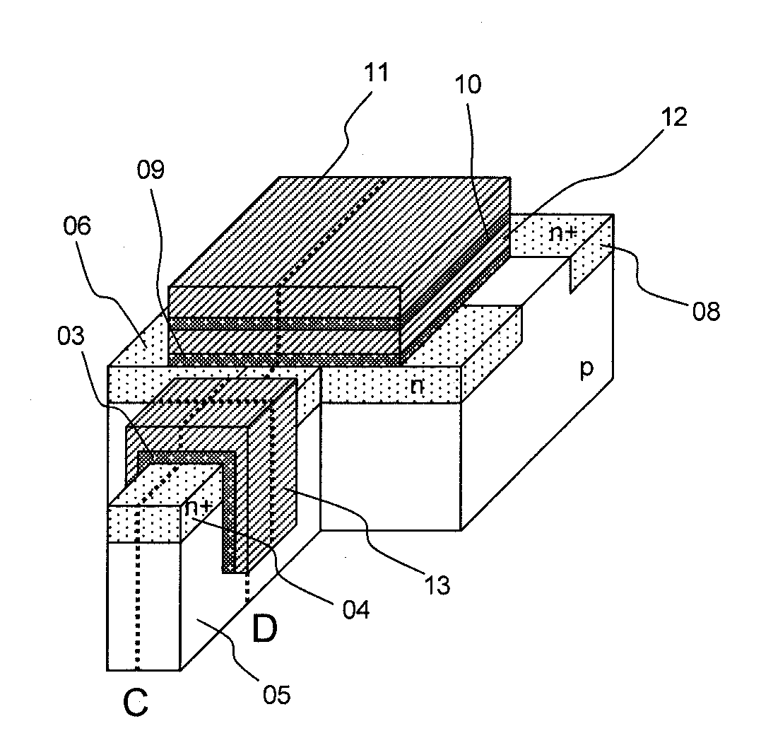
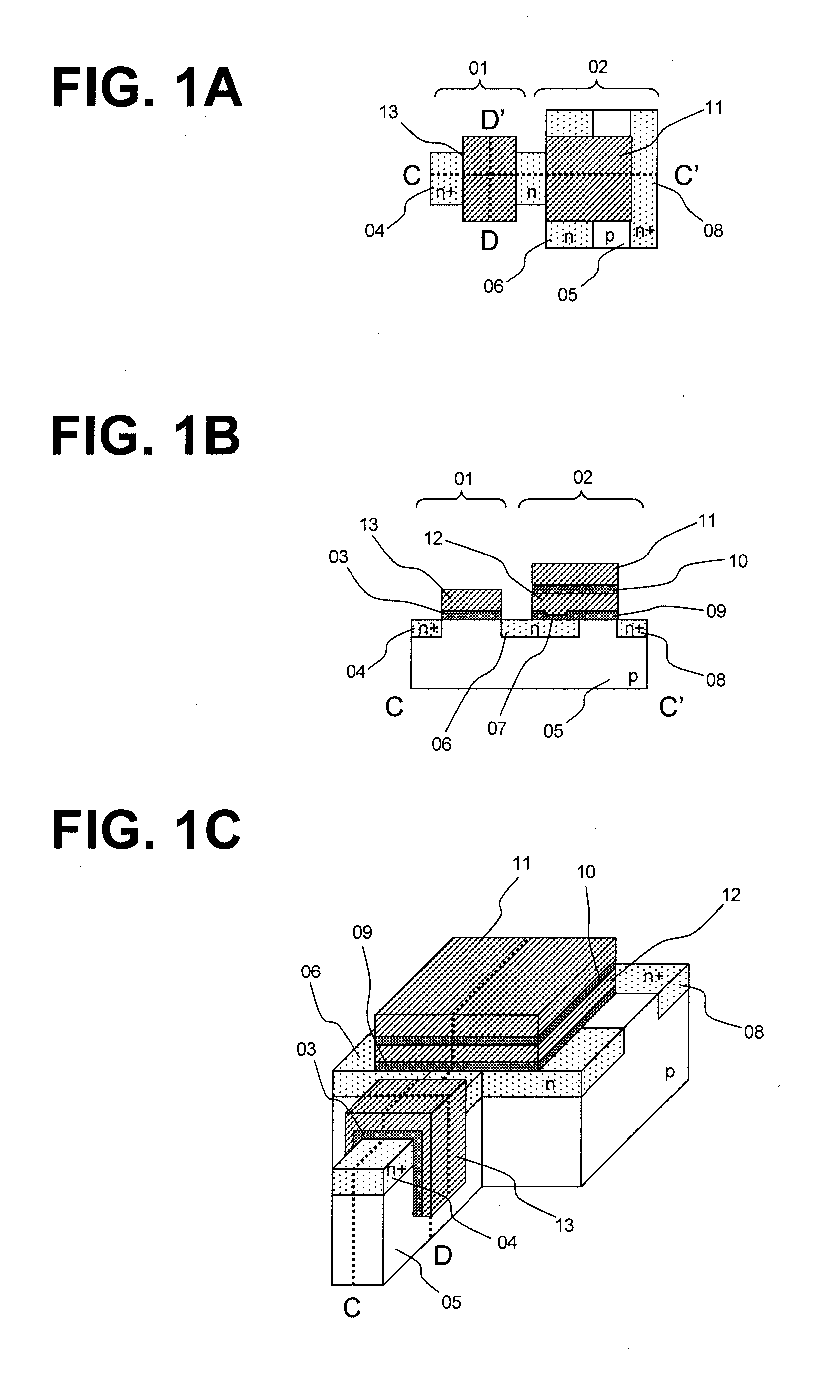
[0042]FIGS. 1A to 1C are diagrams illustrating an EEPROM according to a first embodiment of the present invention. FIG. 1A is a plan view, FIG. 1B is a sectional view taken along the line C-C′, and FIG. 1C is a perspective view.
[0043]The EEPROM of the present invention includes, similarly to the related-art EEPROM that is illustrated in FIGS. 8A to 8C, a memory main body portion 02 and a select gate transistor portion 01 for selecting the memory main body portion 02. The basic operation principle of the EEPROM of FIGS. 1A to 1C is the same as that of the related-art EEPROM described above, and the sectional view of FIG. 1B is also the same as FIG. 8B. The difference is that the select gate transistor portion 01 of the present invention is formed of a fin-shaped single-crystal semiconductor thin film that stands like a wall.
[0044]The select gate transistor portion 01 is formed of a fin-shaped single-crystal semiconductor thin film created by a process in which a p-type silicon substr...
second embodiment
[0049]A second embodiment of the present invention is described with reference to FIGS. 3A to 3C. The second embodiment is a modification of the EEPROM of FIGS. 1A to 1C according to the first embodiment, and is obtained by forming the memory main body portion 02 into a fin shape as well. FIG. 3A is a plan view, FIG. 3B is a sectional view taken along the line E-E′, and FIG. 3C is a perspective view. Sectional views of the structure of FIGS. 3A to 3C that are taken along the line C-C′, which runs from the drain n+ region 04 of FIGS. 1A to 1C toward the source n+ region 08, and the line D-D′, which runs along the width direction of the select gate, are the same as those in the first embodiment, and are therefore omitted.
[0050]As illustrated in FIG. 3A, the memory main body portion 02 in this embodiment is formed on surfaces of a fin-shaped single-crystal semiconductor thin film, which forms the p-type silicon substrate 05 thinned to have the same thickness as that of the select gate ...
third embodiment
[0052]A method of manufacturing the EEPROM of the first embodiment that has a fin shape only in the select gate is described next with reference to FIGS. 4A to 4D.
[0053]First, ion implantation or the like is used to form a plurality of n− regions 20 in parallel on the p-type semiconductor substrate 05 as illustrated in FIG. 4A. The notation “n−” indicates the relative level of the n-type impurity concentration, which satisfies a relation n−+. Thereafter, a plurality of trenches that can serve as shallow trench isolation (STI) regions are formed so as to be orthogonal to the n− regions 20. STI internal oxide films 17 are embedded in concave portions of the trenches. The step of forming the n regions and the step of forming the STI regions may be switched with each other in the order.
[0054]Next, as illustrated in FIG. 4B, the STI internal oxide films 17 are partially removed by etching to form a fin-shaped single-crystal semiconductor thin film. The select gate is formed along the reg...
PUM
 Abstract
Description
Claims
Application Information
PatSnap Eureka turns technology decisions into work you can execute. Powered by our Innovation Knowledge Graph, it runs expert workflows across engineering, life sciences, materials and intellectual property. Get your review-ready output in minutes.


