Electronic device, performance binning system and method, voltage automatic calibration system
- Summary
- Abstract
- Description
- Claims
- Application Information
AI Technical Summary
Benefits of technology
Problems solved by technology
Method used
Image

Examples
Embodiment Construction
[0025]Reference will now be made in detail to the present embodiments of the disclosure, examples of which are illustrated in the accompanying drawings. Wherever possible, the same reference numbers are used in the drawings and the description to refer to the same or like parts.
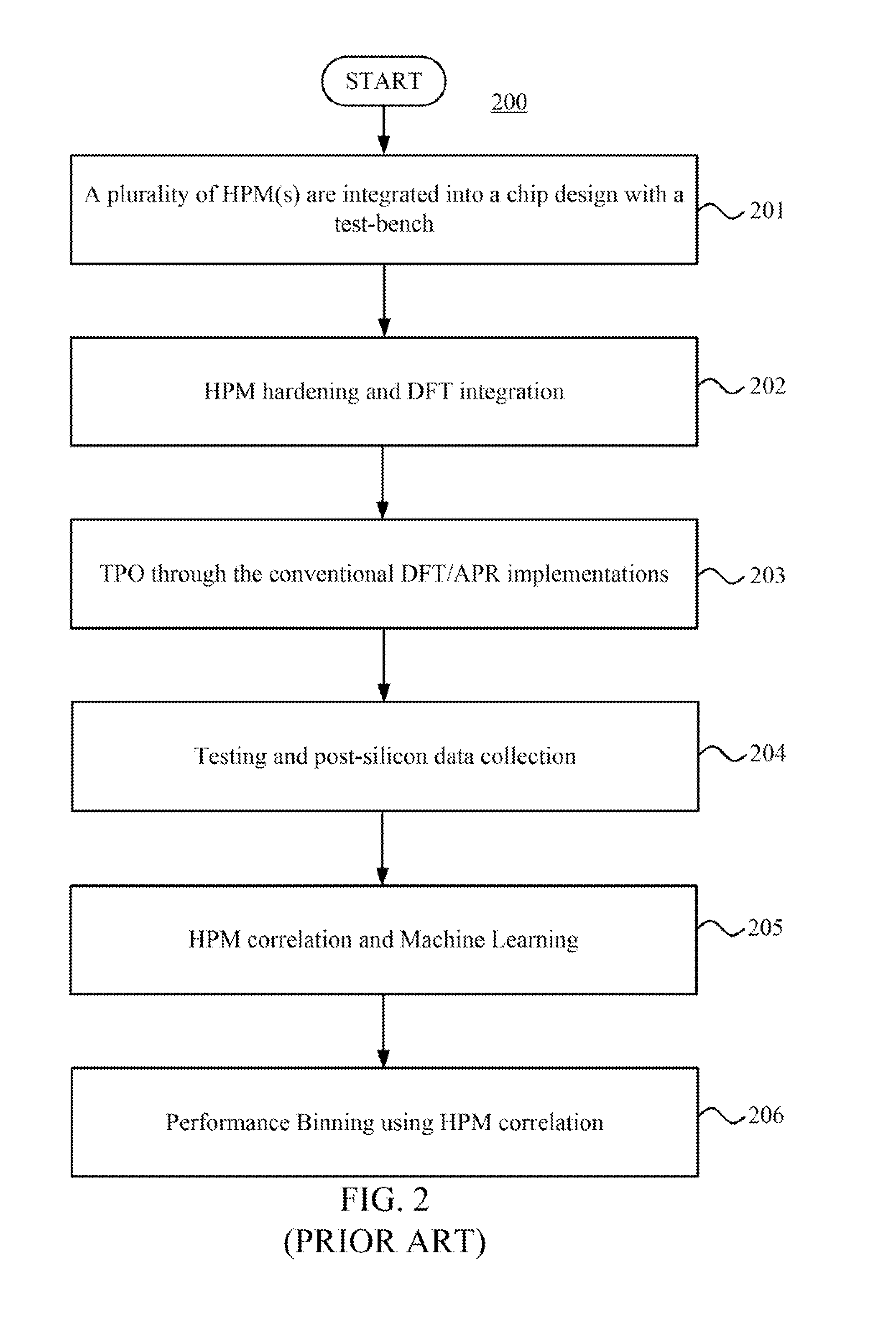
[0026]FIG. 2 illustrates a flow chart of using HPM(s) in a chip to do performance binning automatically through a built-in self-test (BIST) module inside the chip. In step 201, pluralities of HPM(s) are integrated into a chip design with a test-bench to verify the integration, which can be compiled by a HPM complier. In step 202, HPM(s) hardening and OFT integration can be performed. In step 203, the chip can be tapped out after all the design has been layout and verified. In step 204, after the chip is fabricated, post-silicon testing and HPM(s) data can be collected for further analyses. In step 205, HPM(s) data and performance correlation can be determined by a set of sample chips, in which each of the sam...
PUM
 Abstract
Description
Claims
Application Information
 - Generate Ideas
- Intellectual Property
- Life Sciences
- Materials
- Tech Scout
- Unparalleled Data Quality
- Higher Quality Content
- 60% Fewer Hallucinations
Browse by: Latest US Patents, China's latest patents, Technical Efficacy Thesaurus, Application Domain, Technology Topic, Popular Technical Reports.
© 2025 PatSnap. All rights reserved.Legal|Privacy policy|Modern Slavery Act Transparency Statement|Sitemap|About US| Contact US: help@patsnap.com